Method for manufacturing enhanced gallium nitride power device

A technology of power devices and gallium nitride, which is applied in the direction of semiconductor devices, semiconductor/solid-state device manufacturing, electrical components, etc., can solve problems such as large on-resistance, poor device characteristics, and negative threshold value, so as to reduce the difficulty of the process, The effect of avoiding barrier layer interface damage and improving process efficiency and yield

Active Publication Date: 2020-09-11
HUNAN SANAN SEMICON CO LTD
View PDF6 Cites 0 Cited by
  • Summary
  • Abstract
  • Description
  • Claims
  • Application Information

AI Technical Summary

Problems solved by technology

The difficulty of this method is that the etchant used for dry etching of the p-type nitride layer usually has a corrosive effect on the barrier layer material (commonly AlGaN), so the etching accuracy is extremely high, and it is necessary to maintain the p-type nitride layer. Etching is complete and uniform, and the integrity of the next layer must be ensured, so that the surface of the barrier layer is not damaged; unclean etching and overetching will lead to poor device characteristics, such as large on-resistance or negative threshold value And other issues

Method used


Image

  • Method for manufacturing enhanced gallium nitride power device
  • Method for manufacturing enhanced gallium nitride power device

Examples


Embodiment Construction

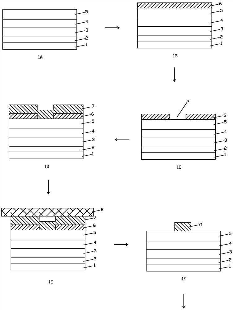
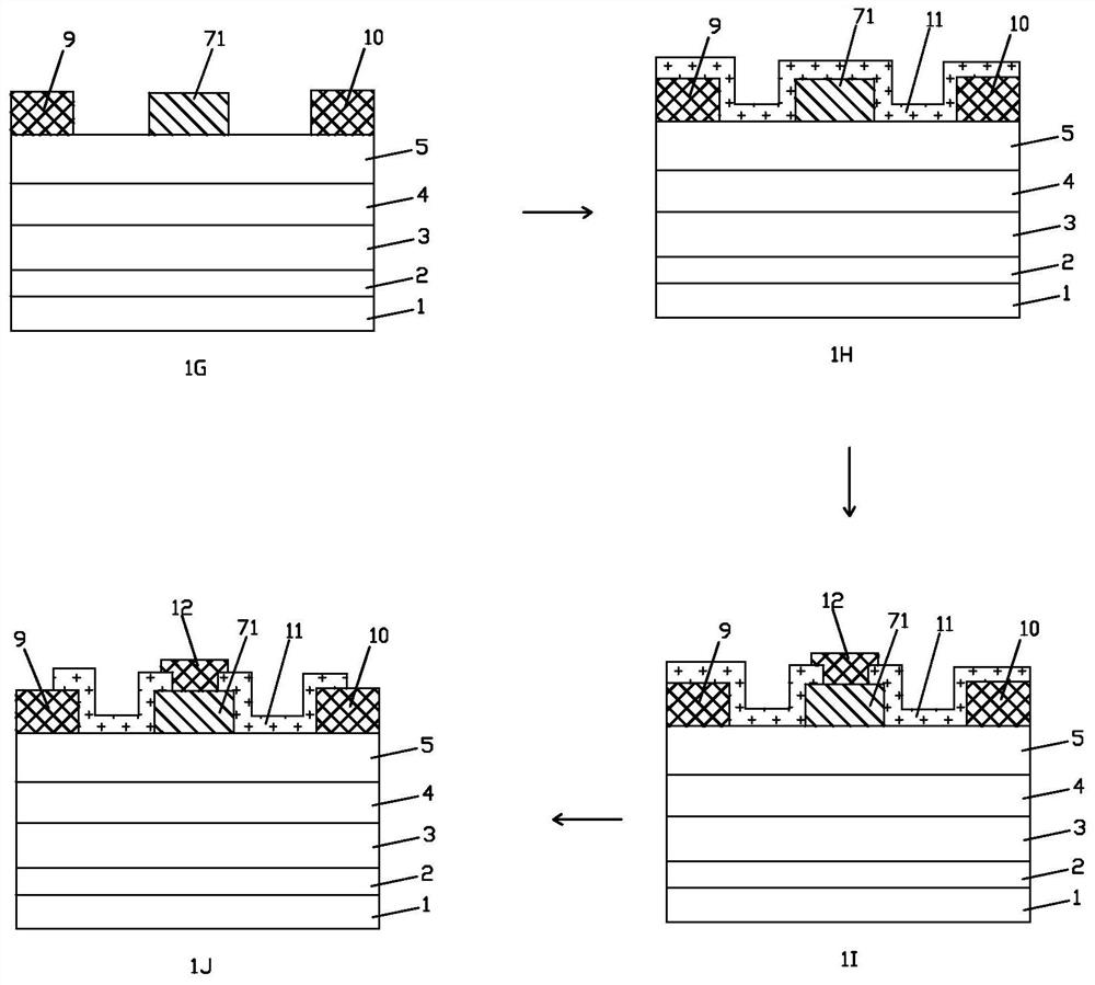
[0031] The present invention will be described in further detail below in conjunction with the accompanying drawings and embodiments. The accompanying drawings of the present invention are only schematic for easier understanding of the present invention, and the specific proportions thereof can be adjusted according to design requirements. Those skilled in the art should understand that the upper and lower relationships of relative components in the figures described herein refer to the relative positions of the components, so all of them can be turned over to present the same components, which should all fall within the scope of the present specification. In addition, the numbers of components and structures shown in the figure are only examples, and are not intended to limit the numbers, and can be adjusted according to actual design requirements.

[0032] refer to figure 1 1A, a semiconductor substrate is provided, and the semiconductor substrate includes an Si substrate 1...


PUM

PropertyMeasurementUnit
thicknessaaaaaaaaaa
thicknessaaaaaaaaaa

Abstract

The invention discloses a method for manufacturing an enhanced gallium nitride power device. The method comprises the steps of forming a layered nano material layer on a barrier layer of a semiconductor substrate, etching the layered nano material layer at a preset grid position to form a first window, depositing a p-type nitride layer, then stripping the layered nano material layer, and forming ap-type grid layer by the p-type nitride layer in the remaining first window. And the layered nano material layer is a hexagonal boron nitride film or a graphene-like two-dimensional nano material. According to the invention, the enhanced gallium nitride power device is manufactured by adopting the layered nano material layer, so that the interface damage of the barrier layer caused by the etchingof the p-type nitride layer is avoided, and the electrical property of the device is improved.

Description

technical field [0001] The invention relates to the technical field of semiconductors, in particular to a method for manufacturing an enhanced gallium nitride power device. Background technique [0002] GaN materials have the characteristics of large bandgap width, high critical breakdown electric field, and high thermal conductivity, and have broad application prospects in broadband communications, power electronics, and other fields. In particular, GaN-based high electron mobility field-effect transistors (HEMTs) are a new class of electronic devices based on nitride heterostructures. The device has excellent characteristics of high frequency and high power, and is widely used in information transmission and reception, energy conversion and other fields such as wireless communication base stations and power electronic devices. [0003] At present, the most common process method for enhancement-mode GaN devices is mainly the p-type nitride gate structure, that is, the p-ty...

Claims


Application Information

Patent Timeline
Patent Type & Authority Applications(China)
IPC IPC(8): H01L21/335H01L29/778H01L29/06
CPCH01L29/66462H01L29/778H01L29/0684
Inventor 梁玉玉蔡文必刘成叶念慈赵杰
Owner HUNAN SANAN SEMICON CO LTD
Why Eureka
Try Eureka