Eureka AIR delivers breakthrough ideas for toughest innovation challenges, trusted by R&D personnel around the world.

Manufacturing method of contact layer, semiconductor laser and manufacturing method of semiconductor laser

A manufacturing method and laser technology, applied in the direction of semiconductor lasers, lasers, laser parts, etc., to achieve the effect of not easy to fall off, good conductivity, and firm adhesion

Active Publication Date: 2020-09-18
SUZHOU EVERBRIGHT PHOTONICS CO LTD +1
View PDF12 Cites 3 Cited by
  • Summary
  • Abstract
  • Description
  • Claims
  • Application Information

AI Technical Summary

Problems solved by technology

[0005] Therefore, the technical problem to be solved by the present invention is to overcome the problem that the semiconductor laser in the prior art is provided with a layer of dielectric film between the electrode and the wafer in order to realize the non-uniform injection of carriers, thus causing the electrode to adhere to the wafer. Defects of poor performance and easy to fall off electrodes

Method used


Image

  • Manufacturing method of contact layer, semiconductor laser and manufacturing method of semiconductor laser
  • Manufacturing method of contact layer, semiconductor laser and manufacturing method of semiconductor laser
  • Manufacturing method of contact layer, semiconductor laser and manufacturing method of semiconductor laser

Examples


Embodiment 1

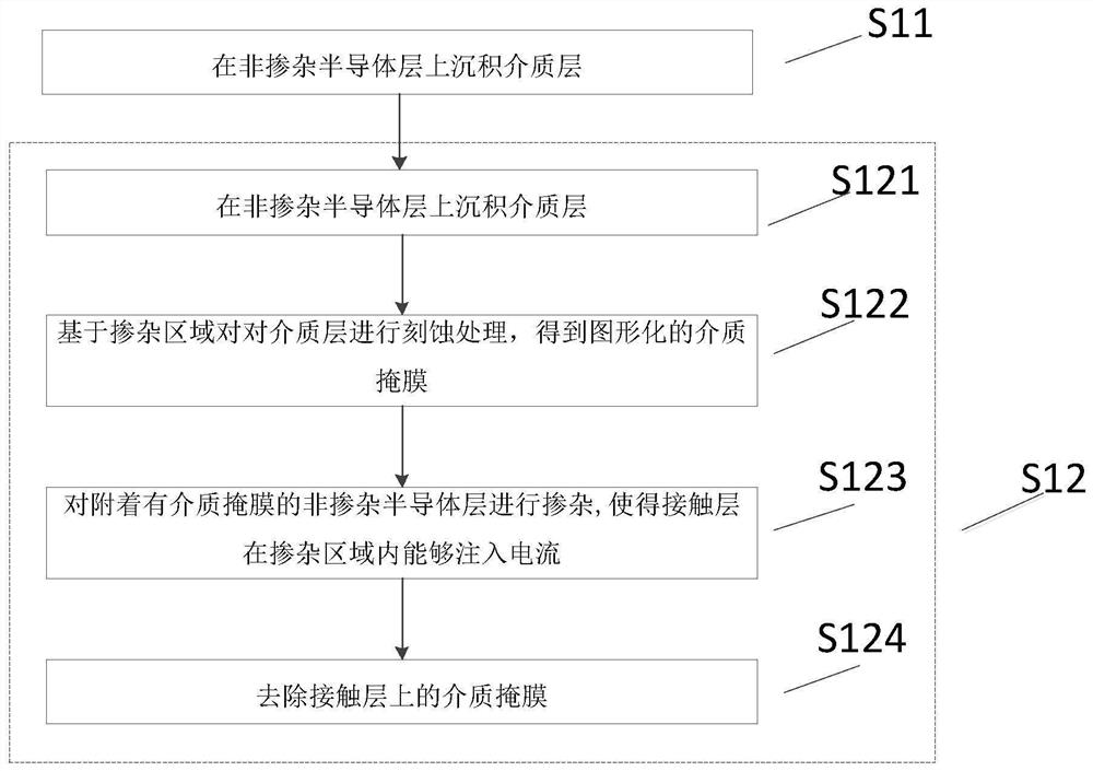
[0051] This embodiment provides a method for manufacturing a contact layer of a semiconductor laser, such as figure 1 with figure 2 shown, including the following steps:

[0052] S11: forming a non-doped semiconductor layer on the epitaxial layer of the semiconductor laser. Specifically, a non-doped GaAs semiconductor layer is grown on the epitaxial layer of the semiconductor laser in a Metal-organic Chemical Vapor Deposition (MOCVD) device, such as image 3 As shown, for example, the non-doped GaAs semiconductor layer has a thickness of 400 nm.

[0053] S12: Doping the non-doped semiconductor layer to form a contact layer having a doped region 101 capable of injecting current. Along the cavity length direction (ie Image 6 The y-axis direction in ) divides the doped region 101 into several sections, and the area of ​​the small doped region 101 in each section is the area capable of injecting current in the doped region 101 . The area capable of injecting current in the ...

Embodiment 2

[0065] This embodiment provides a method for manufacturing a semiconductor laser, comprising the following steps:

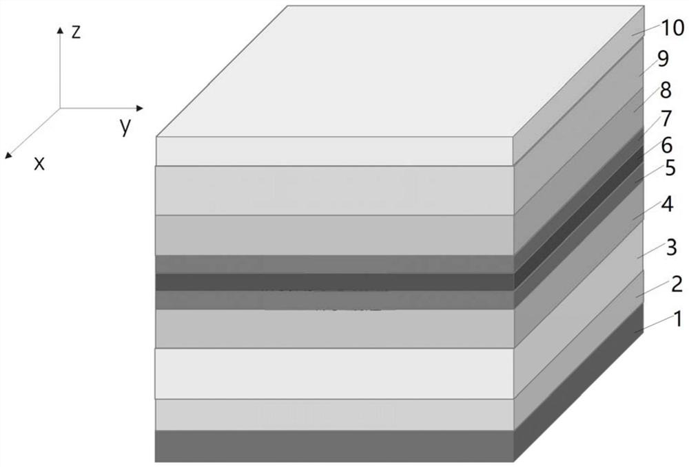
[0066] S21: Generating an epitaxial layer of the semiconductor laser. Specifically, an N-type GaAs (gallium arsenide) substrate 1 is first grown in the MOCVD equipment, and then an N-type GaAs buffer layer 2 and an N-type AlGaAs (aluminum gallium arsenide) lower limit layer are sequentially grown on the N-type GaAs substrate 1 . Layer 3, N-type AlGaAs lower waveguide layer 4, GaAs quantum barrier layer 5, InGaAs (indium gallium arsenide) quantum well layer 6, GaAs quantum barrier layer 7, P-type AlGaAs upper waveguide layer 8, P-type AlGaAs upper confinement layer 9 , the epitaxial layer includes the above layers except the N-type GaAs substrate 1 .

[0067] S22: Using the manufacturing method described in Embodiment 1 to generate a contact layer to obtain a semiconductor laser structure including the contact layer. The semiconductor laser structure includes an...

Embodiment 3

[0073] This embodiment provides a semiconductor laser, see Figure 7 , which includes a semiconductor laser structure, electrodes formed on the upper and lower surfaces of the semiconductor laser structure, and anti-reflection films 132 and anti-reflection films 131 on the left and right sides of the semiconductor laser structure.

[0074] Wherein, the semiconductor laser structure includes an N-type GaAs substrate 1, an epitaxial layer and a contact layer. The epitaxial layer includes N-type GaAs buffer layer 2, N-type AlGaAs lower confinement layer 3, N-type AlGaAs lower waveguide layer 4, GaAs quantum barrier layer 5, InGaAs quantum well layer 6, GaAs quantum barrier layer 7, and P-type AlGaAs upper waveguide layer 8 and P-type AlGaAs upper confinement layer 9.

[0075] The electrodes include a P electrode 122 and an N electrode 121 , the P electrode 122 is located under the N-type GaAs substrate 1 , and the N electrode 121 is located above the GaAs contact layer 10 .

[...


PUM

PropertyMeasurementUnit
Thicknessaaaaaaaaaa
Thicknessaaaaaaaaaa

Abstract

The invention provides a manufacturing method of a contact layer, a semiconductor laser and a manufacturing method of the semiconductor laser, and the manufacturing method of the contact layer comprises the following steps: firstly, forming a non-doped semiconductor layer on an epitaxial layer of the semiconductor laser, and then doping the non-doped semiconductor layer. The contact layer manufactured by adopting the manufacturing method comprises a doped region and a non-doped region, the current cannot be injected into the non-doped region; only the doped region can be injected with current;the area of injected current in the doped region is gradually increased along the length direction of the cavity; therefore, influence of uneven distribution of carrier density and gain along the direction from a reflection enhanced film to an antireflection film due to uneven distribution of photon density in the resonant cavity is counteracted, carriers are evenly distributed in the cavity length direction, and the output power and performance stability of the semiconductor laser are improved. An electrode of the semiconductor laser is directly manufactured on the contact layer, no dielectric film is arranged between the electrode and the contact layer, and the electrode and the contact layer are firmly adhered and are not easy to fall off.

Description

technical field [0001] The invention relates to the technical field of semiconductor lasers, in particular to a manufacturing method of a contact layer, a semiconductor laser and a manufacturing method thereof. Background technique [0002] Semiconductor laser is an important optoelectronic device, which can convert injected carriers into photons by radiative recombination. Traditional semiconductor lasers use uniform injection of carriers, that is, carriers are evenly distributed along the entire electrode direction. Semiconductor lasers often use an asymmetric coating method, that is, an AR coating is deposited on one end of the cavity surface for reflected light, and an anti-reflection coating is deposited on the other end of the cavity surface for transmitted light. When the semiconductor laser is in the lasing state, the distribution of the optical field in the cavity will be affected by this asymmetric coating, that is, the photon density in the resonant cavity of the...

Claims


Application Information

Patent Timeline
IPC IPC(8): H01S5/042H01S5/028
CPCH01S5/028H01S5/0287H01S5/0421H01S5/04256
Inventor 程洋王俊谭少阳潘华东廖新胜
Owner SUZHOU EVERBRIGHT PHOTONICS CO LTD
Why Eureka
Eureka Blog
Learn More