Laser and its manufacturing method

A manufacturing method and laser technology, applied to lasers, laser components, semiconductor lasers, etc., can solve the problems of inability to change the shape of the mode field, increase the packaging cost, and mismatch of the mode field, so as to reduce the divergence angle of the far field and increase the Effect of high output power and reduced power density

Active Publication Date: 2022-03-29
INST OF SEMICONDUCTORS - CHINESE ACAD OF SCI
View PDF0 Cites 0 Cited by
  • Summary
  • Abstract
  • Description
  • Claims
  • Application Information

AI Technical Summary

Problems solved by technology

When the light of the semiconductor active device is directly coupled into the optical fiber or the light transmitted by the optical fiber is coupled into the semiconductor active device, the coupling loss may be as high as 10dB due to the mismatch of the mode field between the optical fiber and the semiconductor active device
The coupling efficiency between them can be improved by using lenses or tapered fibers, but these solutions still have the problem of mode field mismatch
These solutions can only change the size of the mode field but cannot change the shape of the mode field, and the alignment tolerance is small, which undoubtedly increases the packaging cost

Method used


Image

  • Laser and its manufacturing method
  • Laser and its manufacturing method
  • Laser and its manufacturing method

Examples


Embodiment 1

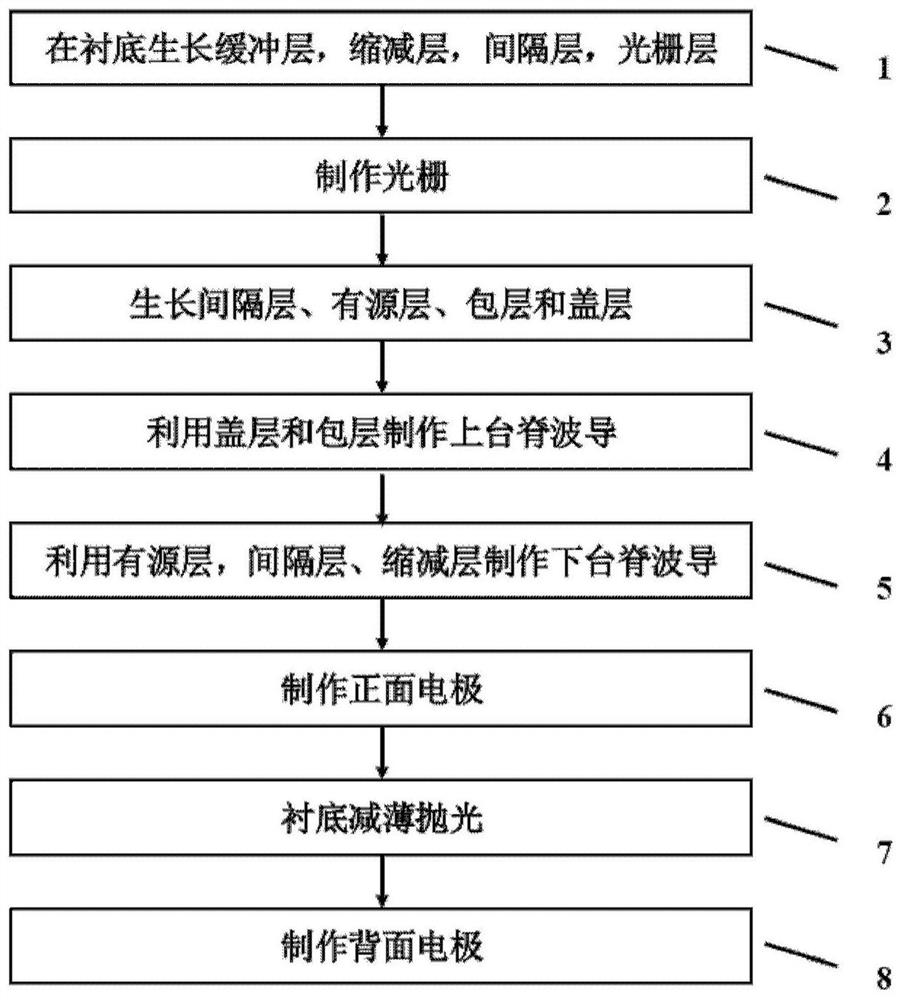
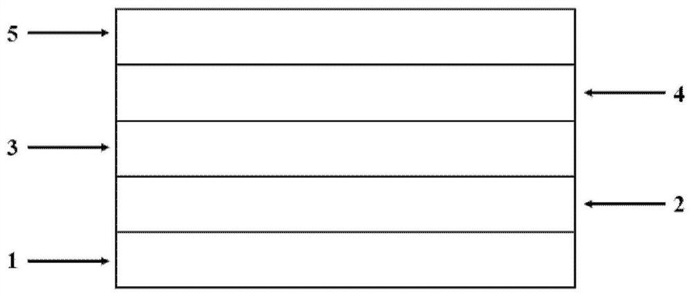
[0065] figure 1 It is a schematic flow chart of the laser manufacturing method in Embodiment 1 of the present invention. Such as figure 1 As shown, step 1: using Metal-organic Chemical Vapor Deposition (MOCVD) to sequentially epitaxially grow an n-type InP buffer layer 2 with a thickness of 500-1000 nm on an n-type InP substrate 1, and a light spot magnification layer 3, 20 ~50nm thick InP spacer layer 4, 30nm thick InGaAsP grating layer 5, such as figure 2 ;

[0066] Wherein, the spot enlargement layer 3 is a far-field reduction layer formed of an InGaAsP layer with a thickness of 40-60 nm;

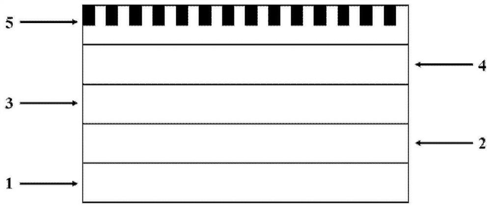
[0067] Step 2: Use holographic exposure technology and dry etching technology to make a large-area grating on the InGaAsP grating layer 5; use holographic exposure to make a uniform grating, and use Reactive Ion Etching (RIE) to etch the grating layer. Soak in grating bromine to repair damage caused by RIE etching, such as image 3 ;

[0068] Step 3: Secondary epitaxial growth of ...

Embodiment 2

[0075] The manufacturing method of this embodiment 2 is the same as that of embodiment 1, the difference is that the light spot amplification layer 3 of this embodiment 2 is a diluted waveguide layer, and a 60nm-thick InGaAsP layer and a 300nm-thick InP layer are alternately grown for 3 to 5 cycles form.


PUM

PropertyMeasurementUnit
thicknessaaaaaaaaaa
thicknessaaaaaaaaaa

Abstract

A laser and a manufacturing method thereof, the laser comprising: a substrate and a double-ridge waveguide; wherein the double-ridge waveguide includes a lower-stage ridge waveguide and an upper-stage ridge waveguide; wherein the lower-stage ridge waveguide is formed on the substrate, It includes a spot enlargement layer, a first spacer layer, a grating layer, a second spacer layer, and an active layer from bottom to top; the upper mesa ridge waveguide is formed on the lower mesa ridge waveguide, and includes a cladding layer and a cover layer from bottom to top; The above-mentioned ridge waveguide includes two sections of wedge-shaped waveguides and one section of straight waveguides, and the two sections of wedge-shaped waveguides are respectively distributed at both ends of the straight waveguide. The invention realizes a high-power laser, improves the coupling efficiency between the laser and the optical fiber, and effectively reduces power consumption and cost.

Description

technical field [0001] The invention relates to the field of optoelectronic devices, in particular to a laser and a manufacturing method thereof. Background technique [0002] As another great invention after computers and semiconductors since the 20th century, laser has the advantages of high brightness, good directionality, and strong coherence. Long-distance, ultra-long-distance, high-speed, ultra-high-speed, and ultra-large-capacity optical fiber communication systems are the needs of the development of modern information society. Whether it is the backbone network and wide area network of long-distance communication, or the local area network of short-distance communication, access network, short-distance data connection optical switching, etc., a large number of high-performance and low-cost optoelectronic devices are required to support the functions of optical networks. Compared with other lasers, semiconductor lasers have the advantages of small size, high efficien...

Claims


Application Information

Patent Timeline
Patent Type & Authority Patents(China)
IPC IPC(8): H01S5/227H01S5/30H01S5/125
CPCH01S5/2275H01S5/3013H01S5/125
Inventor 剌晓波梁松唐强刘云龙张立晨朱旭愿
Owner INST OF SEMICONDUCTORS - CHINESE ACAD OF SCI
Why Eureka
Try Eureka