A kind of lnoi mode spot converter and preparation method based on subwavelength grating

A technology of sub-wavelength grating and mode-spot converter, which is applied in the direction of optical waveguide light guide, optical waveguide coupling, instrument, etc., can solve problems such as difficult LNOI optical chip production, limited optical mode field amplification ability, and weakened limitation ability, etc., to achieve Promote practical application, reduce effective refractive index, and reduce the effect of refractive index difference

Active Publication Date: 2022-05-13
NO 55 INST CHINA ELECTRONIC SCI & TECHNOLOGYGROUP CO LTD
View PDF5 Cites 0 Cited by
  • Summary
  • Abstract
  • Description
  • Claims
  • Application Information

AI Technical Summary

Problems solved by technology

[0003] Mode-spot converters mainly include grating couplers and end-face couplers. The existing end-face couplers mostly use tapered waveguide structures. As the width of the waveguide becomes narrower, the ability of the waveguide to limit the optical mode is also weakened. The core layer of the waveguide The mode field will diffuse into the cladding layer. If a cladding layer with a refractive index similar to that of the waveguide core layer is used, the optical mode field can be further amplified. However, the tapered waveguide is generally relatively long, and the ability to amplify the optical mode field is limited.
The end-face coupler using cantilever beam and three-dimensional tapered waveguide improves the coupling efficiency, but its manufacturing process is difficult and the stability is poor, so it is difficult to realize large-scale LNOI optical chip production

Method used


Image

  • A kind of lnoi mode spot converter and preparation method based on subwavelength grating
  • A kind of lnoi mode spot converter and preparation method based on subwavelength grating
  • A kind of lnoi mode spot converter and preparation method based on subwavelength grating

Examples


preparation example Construction

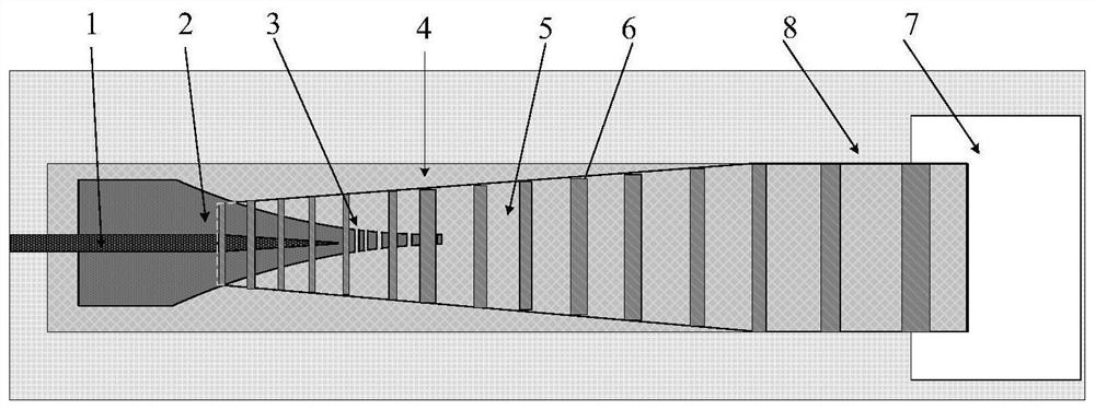
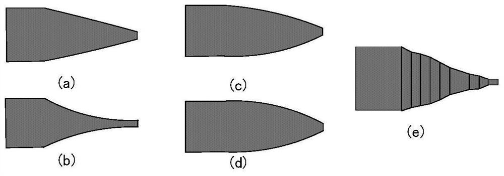
[0054] Such as Image 6 Shown is the processing steps of the preparation method of the LNOI mold spot converter of the present invention, comprises the following steps:

[0055] In step s1, an etching mask for the tapered waveguide 1 on the top layer is prepared. The waveguide etching mask includes photoresist and metal mask. The photoresist includes HSQ negative resist, ZEP 520A positive resist and 7908 positive resist. The material of the metal mask is Ni or Ti / Ni, or Cr / Ni.

[0056] In step s2, the tapered waveguide 1 on the top layer is etched. Waveguide etching adopts dry etching process, reactive ion etching or inductively coupled plasma etching, and the etching gas is Ar, or SF 6 / Ar mixed gas.

[0057] In step s3 , an etching mask for the underlying tapered waveguide 2 and the tapered subwavelength grating 3 is prepared.

[0058] In step s4, the underlying tapered waveguide 2 and the tapered sub-wavelength grating 3 are etched.

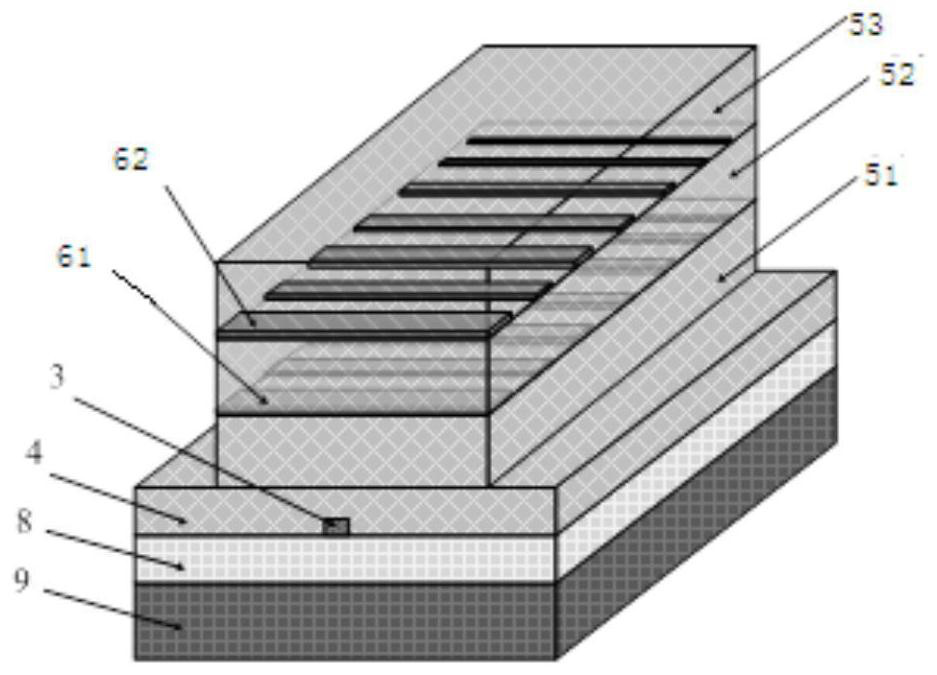
[0059] Step s5, SiO 2 Dielectric ...

Embodiment 1

[0067] A 3-inch x-cut LNOI wafer is selected, the thickness of the lithium niobate film is 600nm, and the SiO 2 The thickness of the insulating layer is 2 μm, the substrate is Si material, and the preparation process steps are:

[0068] A1) Preparation of etching mask for the tapered waveguide 1 on the top layer: Spin-coat the negative resist HSQ at a speed of 2000 rpm / min, and bake on a hot plate at 150°C for 120 seconds.

[0069] A2) Etching of the tapered waveguide 1 on the top layer: Ar plasma ICP etching, the etching depth of the waveguide is 300nm.

[0070] A3) Preparation of the etching mask of the bottom tapered waveguide 2 and the tapered subwavelength grating 3: spin-coat the negative resist HSQ at a speed of 2000 rpm / min, and bake on a 150° C. hot plate for 120 seconds.

[0071] A4) Etching of the bottom tapered waveguide 2 and the tapered subwavelength grating 3: Ar plasma ICP dry etching is used, and the waveguide etching depth is 300 nm.

[0072] A5) First SiO2...

Embodiment 2

[0080] A 3-inch x-cut LNOI wafer is selected, the thickness of the lithium niobate film is 600nm, and the SiO 2 The thickness of the insulating layer is 2 μm, and the substrate is made of Si material. The main preparation process steps are:

[0081] B1) Preparation of etching mask for top-layer tapered waveguide 1: spin-coat photoresist 7908, evaporate metal Ti / Ni20 / 150nm after exposure and development, soak in acetone, remove photoresist by ultrasonication, and then ultrasonically in ethanol for 5 minutes, then Rinse with deionized water, and finally put it in the dryer to dry.

[0082] B2) Etching of the tapered waveguide 1 on the top layer: Ar plasma ICP etching, the etching depth of the waveguide is 300nm.

[0083] B3) Preparation of bottom tapered waveguide 2 and sub-wavelength grating 3 etching mask: spin-coat photoresist 7908, evaporate metal Ti / Ni 20 / 150nm after exposure and development, soak in acetone, remove photoresist by ultrasonic, and then wash in ethanol Ultr...


PUM

PropertyMeasurementUnit
widthaaaaaaaaaa
thicknessaaaaaaaaaa
widthaaaaaaaaaa

Abstract

The invention discloses an LNOI mode speckle converter based on a sub-wavelength grating, comprising: a top-layer tapered waveguide, a bottom-layer tapered waveguide, a tapered sub-wavelength grating, SiO 2 Inverted tapered thick ridge waveguide cladding, SiN subwavelength grating thin layer and fiber fixing groove; the processes involved in the preparation method include: preparation of the top tapered waveguide and bottom tapered waveguide, preparation of tapered subwavelength grating, SiO 2 Preparation of inverted tapered thick ridge waveguide, SiN sub-wavelength grating, and fiber fixing groove. The present invention adopts double-layer tapered waveguide combined with tapered sub-wavelength grating, SiN sub-wavelength grating and SiO 2 The structure of the inverted tapered thick ridge waveguide realizes the amplification function of the small-sized optical mode field in the LNOI optical waveguide by adjusting the effective refractive index of the waveguide core and cladding, thereby improving the coupling efficiency between the LNOI optical waveguide and the single-mode fiber.

Description

technical field [0001] The invention relates to an LNOI mode spot converter and a preparation method, in particular to an LNOI mode spot converter based on a subwavelength grating and a preparation method. Background technique [0002] Thin-film lithium niobate (LNOI, Lithium Niobate on Insulator) material is a new optoelectronic integrated material, its structure is similar to SOI (Silicon on Insulator), which is a three-layer structure, and the top layer of lithium niobate thin film has high electro-optical The advantage of the coefficient is that it is the first choice material for the preparation of high-speed electro-optic modulators and optical switches. The intermediate insulating layer and lithium niobate have a large refractive index difference (Δn=n LiNbO3 -n SiO2 =2.2-1.44=0.76), which can reduce device size and waveguide transmission loss. There are many choices of substrates, and silicon substrates are the most widely used. [0003] Mode-spot converters mainly...

Claims


Application Information

Patent Timeline
Patent Type & Authority Patents(China)
IPC IPC(8): G02B6/124G02B6/14G02B6/136G02B6/30
CPCG02B6/124G02B6/14G02B6/136G02B6/305G02B2006/1204
Inventor 周奉杰钱广顾晓文唐杰孔月婵
Owner NO 55 INST CHINA ELECTRONIC SCI & TECHNOLOGYGROUP CO LTD
Why Eureka
Try Eureka