Field-effect transistor, display element, image display device, and system
一种场效应晶体管、显示元件的技术,应用在场效应晶体管,能够解决没有提出n型掺杂高迁移率等问题,达到高稳定性、高迁移率的效果
- Summary
- Abstract
- Description
- Claims
- Application Information
AI Technical Summary
Problems solved by technology
Method used
Image

Examples
example 1
[0180]
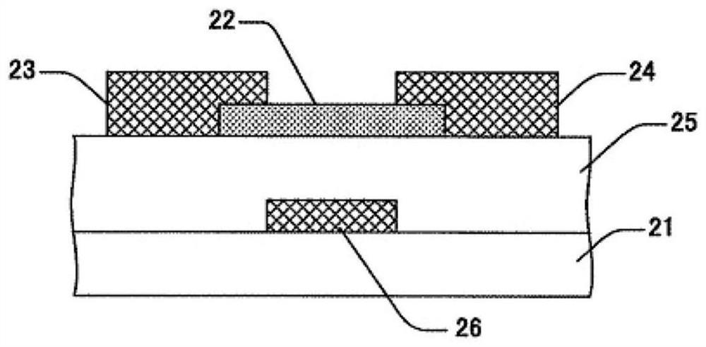
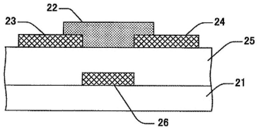
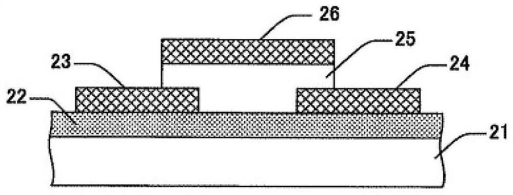
[0181] -Formation of gate electrode-
[0182] Al was vapor-deposited on a glass substrate to have a thickness of 100 nm, and the resulting Al film was patterned into lines by photolithography and etching to form a gate electrode.
[0183] -Formation of gate insulating film-
[0184] Next, at a temperature of 200 °C, the SiH 4 Gas and N 2 O gas was used as a raw material, and a SiON film with a thickness of 200 nm was formed by plasma CVD. The resulting film was used as a gate insulating film.
[0185] -Formation of semiconductor layer-
[0186] Formation of Sn-doped In on the gate insulating film by RF magnetron sputtering 2 o 3 film so as to have a film thickness of 20 nm. The target used is with In 1.96 sn 0.04 o 3 Polycrystalline sintered body of composition. Argon and oxygen were introduced as sputtering gases. The total pressure was fixed at 1.1 Pa, and the oxygen concentration was set at 50% by volume. Patterning is performed by film formation thr...
PUM
| Property | Measurement | Unit |
|---|---|---|
| width | aaaaa | aaaaa |
Abstract
Description
Claims
Application Information
 - R&D
- Intellectual Property
- Life Sciences
- Materials
- Tech Scout
- Unparalleled Data Quality
- Higher Quality Content
- 60% Fewer Hallucinations
Browse by: Latest US Patents, China's latest patents, Technical Efficacy Thesaurus, Application Domain, Technology Topic, Popular Technical Reports.
© 2025 PatSnap. All rights reserved.Legal|Privacy policy|Modern Slavery Act Transparency Statement|Sitemap|About US| Contact US: help@patsnap.com