Supercharge Your Innovation With Domain-Expert AI Agents!

Plating hanger and processing method for BGA packaged circuit module

A technology for encapsulating circuits and circuit modules, applied in printed circuits, printed circuit manufacturing, electrolytic components, etc., can solve the problems of nickel plating and gold plating solution waste, damage to the surface of potting body, incomplete coating, etc., to ensure reliability and Uniformity, convenient and precise positioning, and the effect of ensuring continuity

Active Publication Date: 2021-05-25
XIAN MICROELECTRONICS TECH INST
View PDF7 Cites 0 Cited by
  • Summary
  • Abstract
  • Description
  • Claims
  • Application Information

AI Technical Summary

Problems solved by technology

[0006] 2. Hanging basket: The surface of the hanging basket will also be electroplated with nickel layer during the electroplating and electroplating process of the hanging basket. In the later electroplating process of nickel and gold, due to the large surface area of ​​the hanging basket, the waste of nickel plating and gold plating solution is too large; And in the process of nickel-gold electroplating, if the surface to be plated touches the hanging basket, there will be local coating defects and burnt phenomena on the electroplated surface of the contact part, and the appearance of the processed product does not meet the requirements;
[0008] 4. Binding method: Use fine copper wire to bind the product, but in the process of binding with copper wire, the loosely bound product is easy to fall off, and the tightly bound product will damage the surface of the potting body and form defects, and after electroplating, local coatings will be formed at the edges and corners incomplete problem
When electroplating traditional packaging (SOP, etc.) circuits, the external lead frame is generally used as the contact point with the hanger. Since the BGA package circuit has no external leads protruding, there is no hanging and conductive point during the surface metallization process. Hanging plating is not possible, and methods such as hanging baskets and binding cannot meet the requirements of complete and uniform plating

Method used


Image

  • Plating hanger and processing method for BGA packaged circuit module
  • Plating hanger and processing method for BGA packaged circuit module
  • Plating hanger and processing method for BGA packaged circuit module

Examples


Embodiment

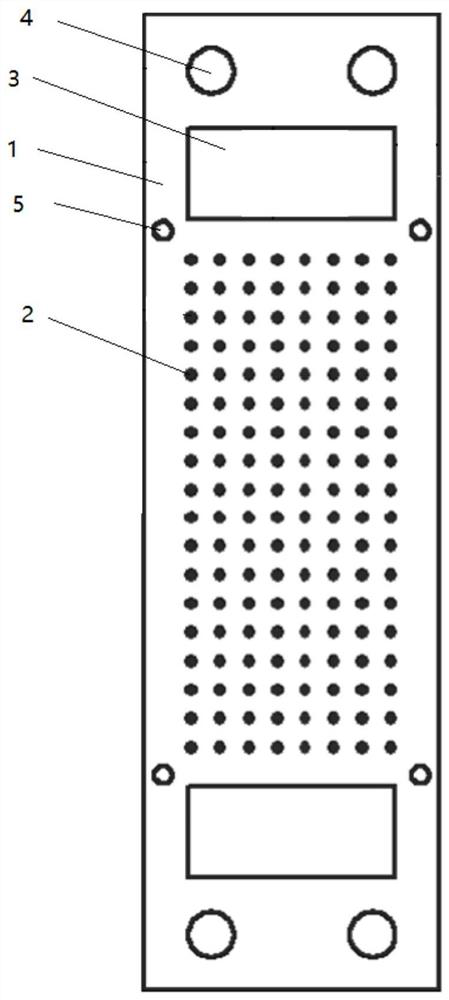
[0042] by figure 2 Taking the BGA package circuit module as an example, design the hanger:

[0043] 1. figure 2 The size of the BGA pad on the bottom board of the circuit module is 0.76mm, and the surface of the bottom board is coated with solder resist. Set the surface contact point at the corresponding position, the size of the contact point is 0.56mm (0.1mm smaller than one side of the pad), and select the first row and two columns, one row and 11 columns, 20 rows and two columns, and 20 rows and 11 columns of the BGA pad on the bottom board , the corresponding positions of the 4 pads are provided with alignment holes, the size of the alignment holes is 0.8mm (0.02mm larger than the single side of the pad), and the graphic design of the substrate processing is as follows: figure 1 ;

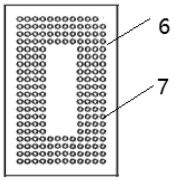
[0044] 2. Design the bending area on both sides of the alignment figure, the center of the bending area is designed to be hollowed out with a width of 2mm on both sides of the connecting ...


PUM

PropertyMeasurementUnit
sizeaaaaaaaaaa

Abstract

The invention discloses a plating hanger and a processing method for a BGA packaged circuit module. The plating hanger of the invention adopts a bendable connecting piece to make the hanger, and a hollowed-out hanger pattern is designed to make the plane process metal After the contact point, the bending and forming processing of the hanger is realized. The bent hanger is fixed on the bottom plate by anti-plating glue, which not only ensures the firmness of the hanger, but also protects the bottom plate from metallization, and at the same time makes it clampable and hookable during the plating process. The contact point avoids the problem of coating defects caused by clamping and hanging on the effective coating surface of the module. In the present invention, the connecting piece is used as a hanger hook, and it is assembled with the BGA circuit before the surface is metallized. The hanger enables the plating process to be clamped, and at the same time, the non-plating surface is protected from plating, ensuring the plating The conductivity of the current during the process, the surface coating of the processed circuit module is complete and the thickness is uniform.

Description

technical field [0001] The invention belongs to the field of electronic electroplating, and in particular relates to a plating hanger and a processing method for BGA packaged circuit modules. Background technique [0002] The BGA package circuit module is to vertically stack the PCB interconnection substrates of multi-layer soldered devices, and use epoxy resin potting compound for overall potting. After curing, the side of the potting body is precisely cut to expose the printed board connection lines. A matrix of interconnection points is formed, and then side interconnection lines are formed through surface plating and laser scribing to complete the three-dimensional assembly and interconnection between substrates. The surface plating is the key condition to realize the interconnection point connection. [0003] The bottom plate and interconnection substrate of the BGA package circuit module are silk screen solder resist on the surface of the FR-4 printed board, and the s...

Claims


Application Information

Patent Timeline
Patent Type & Authority Patents(China)
IPC IPC(8): C25D17/08H05K3/18
CPCC25D17/08H05K3/187
Inventor 陈慧贤杨胜利顾毅欣
Owner XIAN MICROELECTRONICS TECH INST
Features
  • R&D
  • Intellectual Property
  • Life Sciences
  • Materials
  • Tech Scout
  • Unparalleled Data Quality
  • Higher Quality Content
  • 60% Fewer Hallucinations
Learn More