Multi-die FPGAs implementing clock trees using active silicon connection layers

A connection layer, multi-die technology, used in CAD circuit design, special data processing applications, climate sustainability, etc., can solve problems such as large structural limitations, asynchronous clocks, single signal interconnection, etc. Design Convergence, Improved Performance

Active Publication Date: 2022-05-31
WUXI ESIONTECH CO LTD
View PDF6 Cites 0 Cited by
  • Summary
  • Abstract
  • Description
  • Claims
  • Application Information

AI Technical Summary

Problems solved by technology

However, the above two patents are limited by the defects of the chip itself and the structural design. Both of them can only interconnect two adjacent IC dies arranged side by side, and can only realize signal interconnection in a single direction. Very limited
In addition, the balance of cross-die clock signals in this multi-die structure is also a problem that has to be considered, and it is also a big challenge. The conventional approach may be to connect the clock inputs between the die in series, but this It will cause the clock to be out of sync, and the clock skew will be very large, which will seriously affect the performance of cross-die design

Method used


Image

  • Multi-die FPGAs implementing clock trees using active silicon connection layers
  • Multi-die FPGAs implementing clock trees using active silicon connection layers
  • Multi-die FPGAs implementing clock trees using active silicon connection layers

Examples


Embodiment Construction

[0028] The specific embodiments of the present invention will be further described below in conjunction with the accompanying drawings.

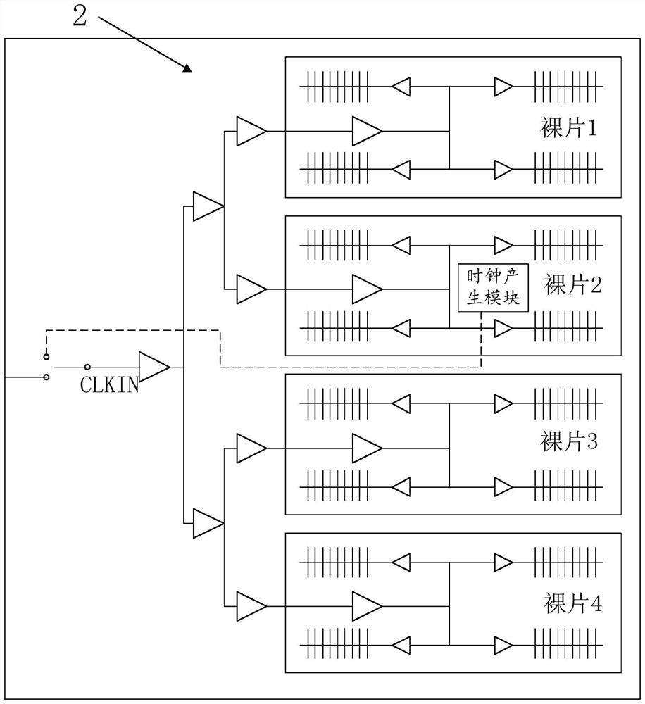
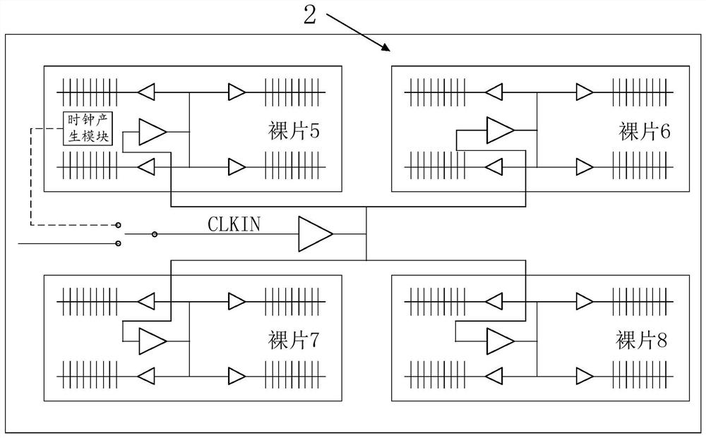
[0045] Each silicon stack connection module also has an interconnection resource module distributed around the silicon stack connection module, because

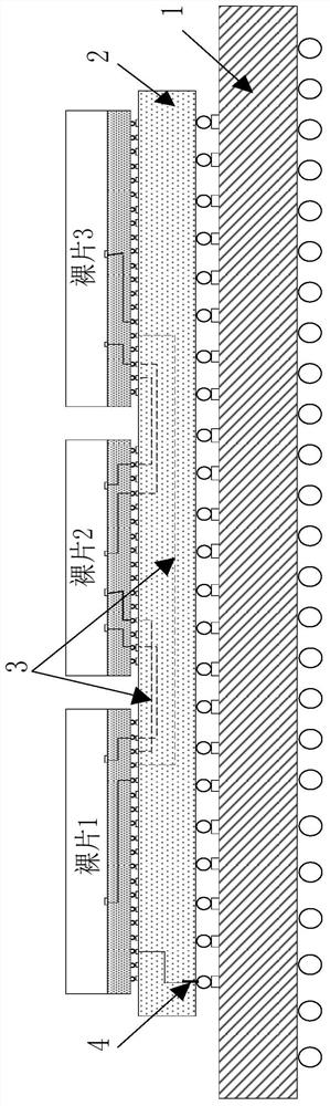
[0047] With this structure, the die signal of the FPGA die has been connected to the connection point terminal 6 by the silicon stack connection point 5 .

[0049] In addition, the inter-die wiring 3 arranged in the silicon connection layer 2 may also intersect along the first direction and the second direction

[0050] The above are only preferred embodiments of the present application, and the present invention is not limited to the above embodiments. It is understandable that this


PUM


Abstract

The present application discloses a multi-die FPGA utilizing an active silicon connection layer to implement a clock tree. The multi-die FPGA includes several FPGA dies, and these several FPGA dies are stacked on the same silicon connection layer. Interconnection communication is realized through the cross-die connection inside the silicon connection layer; source devices are also arranged in the silicon connection layer to build a balanced clock tree, and the clock signal is pushed to each FPGA die through the balanced clock tree, so that the clock of each FPGA die Synchronization, the balanced clock tree in the silicon connection layer can balance the delay of the clock signal reaching each FPGA die, reduce the problem of excessive clock skew in cross-die communication, speed up design convergence, and improve the performance of multi-die FPGAs .

Description

Multi-die FPGAs for Clock Trees Using Active Silicon Link Layers technical field The present invention relates to semiconductor technology field, especially a kind of multi-die utilizing active silicon connection layer to realize clock tree FPGA. Background technique FPGA (Field Programmable Gate Array, Field Programmable Logic Gate Array) is a hardware programmable The programmed logic devices are not only used in mobile communications, data centers and other fields, but also widely used in integrated circuit design. Prototype verification can effectively verify the correctness of circuit functions and speed up circuit design. Prototype verification requires the use of The programmable logic resources inside the FPGA realize circuit design. With the continuous increase in the scale of integrated circuits and the realization of complex functions At present, the demand for the number of programmable logic resources of FPGA continues to increase, and the subsequent ...

Claims


Application Information

Patent Timeline
Patent Type & Authority Patents(China)
IPC IPC(8): G06F30/34
CPCG06F30/34Y02D10/00
Inventor 单悦尔徐彦峰范继聪张艳飞闫华
Owner WUXI ESIONTECH CO LTD
Why Eureka
Try Eureka