A kind of microled preparation method based on three-dimensional mask substrate

A mask and three-dimensional technology, applied in the direction of semiconductor devices, electrical components, circuits, etc., can solve the problems of reducing luminous efficiency, difficult to further reduce costs, increase heat generation, etc., and achieve the effect of improving light emitting efficiency.

Active Publication Date: 2022-03-11
北京飓芯科技有限公司
View PDF5 Cites 0 Cited by
  • Summary
  • Abstract
  • Description
  • Claims
  • Application Information

AI Technical Summary

Problems solved by technology

Because of the small size of the MicroLED, it is intolerable for the local high dislocation density area, because the local high dislocation density will cause the device to be inconsistent with other devices, or even fail completely.
From this point of view, although the high quality of the wing area of ​​ELOG technology can meet the crystal quality requirements of Micro LED, the high dislocation density in the window area is unacceptable.
[0007] 4) In terms of production cost, Micro LED also has strict restrictions
Mass production of Micro LEDs using homogenous substrates is unrealistic because the price is too high for the market to accept
On the other hand, the use of laser lift-off technology, one-by-one electrical inspection and other technologies is also the reason why it is difficult to further reduce the cost
[0008] 5) At present, the mass transfer problem is still an important technical issue for the industrialization of Micro LED. For this reason, researchers at home and abroad have developed a variety of mass transfer methods, but they are all time-consuming and costly.
But the etching process is damaging to the side
Damage to the side wall will lead to a decrease in luminous efficiency, a shift in the luminous wavelength, a decrease in the ability to withstand current, and an increase in heat generation, which need to be avoided as much as possible

Method used


Image

  • A kind of microled preparation method based on three-dimensional mask substrate
  • A kind of microled preparation method based on three-dimensional mask substrate
  • A kind of microled preparation method based on three-dimensional mask substrate

Examples


Embodiment Construction

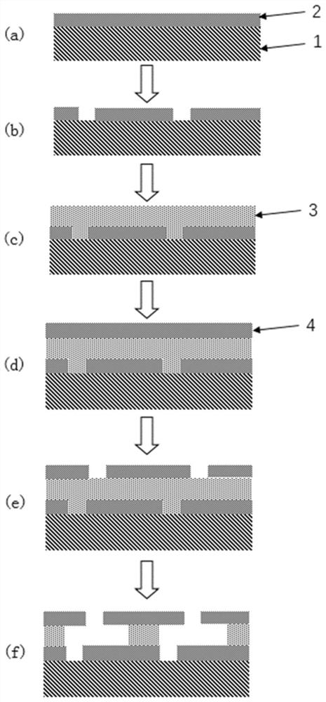
[0046] In order to make the above objects, features and advantages of the present invention more obvious and easy to understand, the present invention will be further described in detail below by taking GaN among III-nitride materials as an example through specific embodiments and accompanying drawings.

[0047] In the present invention, the three-dimensional mask substrate technology used can firstly provide GaN materials with ultra-high crystal quality for the device structure epitaxy of Micro LEDs, thereby solving the demand for high crystal quality in Micro LEDs and overcoming many problems caused by insufficient crystal quality. caused problems. In the second aspect, the three-dimensional mask technology has the characteristics of easy peeling, and the peeled monomer has small protrusions, which is convenient for absorbing and grabbing MicroLEDs during the mass transfer process, which can well meet the needs of MicroLEDs for easy peeling and transfer. . In the third aspe...


PUM

PropertyMeasurementUnit
thicknessaaaaaaaaaa

Abstract

The invention relates to a method for preparing a Micro LED based on a three-dimensional mask substrate. The method prepares a three-dimensional mask layer on a heterogeneous substrate; epitaxially grows a III-nitride material on the heterogeneous substrate by using the three-dimensional mask layer; and epitaxially grows a MicroLED structure on the III-nitride material Floor. This method is aimed at the characteristics of the three-dimensional mask substrate and the high crystal quality requirements of Micro LED. During the growth process on the three-dimensional mask substrate, a pre-stressed layer is inserted in the channel growth stage; SiN is used in the electrode manufacturing process. x Replacement of commonly used SiO 2 As an insulating protective layer; the substrate is peeled off by wet etching; the bottom of the MicroLED is treated with KOH solution to improve the light extraction efficiency.

Description

technical field [0001] The invention belongs to the technical field of micro light-emitting diode displays, and in particular relates to a preparation method of Micro LED based on a three-dimensional mask substrate. Background technique [0002] Micro LED Display (Micro LED Display) is a new generation of display technology. The structure is a miniaturized LED array, that is, the LED structure design is thinned, miniaturized and arrayed, so that its volume is about 1 times the size of the current mainstream LED. %, reaching a size range of 10-30um, each pixel can be addressed and driven to emit light independently, and the distance between pixels is reduced from the original millimeter level to the micron level. Inheriting the characteristics of LED, the advantages of Micro LED include low power consumption, high brightness, ultra-high resolution and color saturation, fast response, super power saving, long life, high efficiency, etc., and its power consumption is about LCD ...

Claims


Application Information

Patent Timeline
Patent Type & Authority Patents(China)
IPC IPC(8): H01L33/00
CPCH01L33/007
Inventor 张晓蓉郑烨琳冯筱陈明兰
Owner 北京飓芯科技有限公司
Why Eureka
Try Eureka