Surface protection film for processing device with uneven structure on surface

A surface protection film and uneven technology, applied in the direction of film/sheet adhesive, non-polymer organic compound adhesive, adhesive, etc., can solve the problems of damage to the concave and convex surface of the device, insufficient strength of the protective film, etc.

Pending Publication Date: 2020-10-27
TAIHU JINZHANG TECH CO LTD
View PDF0 Cites 0 Cited by
  • Summary
  • Abstract
  • Description
  • Claims
  • Application Information

AI Technical Summary

Problems solved by technology

[0003] In the prior art, the strength of the protective film is not enough during the processing of the device. When the device is subjected to mechanical operations such as high-intensity grinding, it is easy to cause damage to the concave-convex surface of the device.

Method used


Image

  • Surface protection film for processing device with uneven structure on surface
  • Surface protection film for processing device with uneven structure on surface
  • Surface protection film for processing device with uneven structure on surface

Examples


Embodiment 1

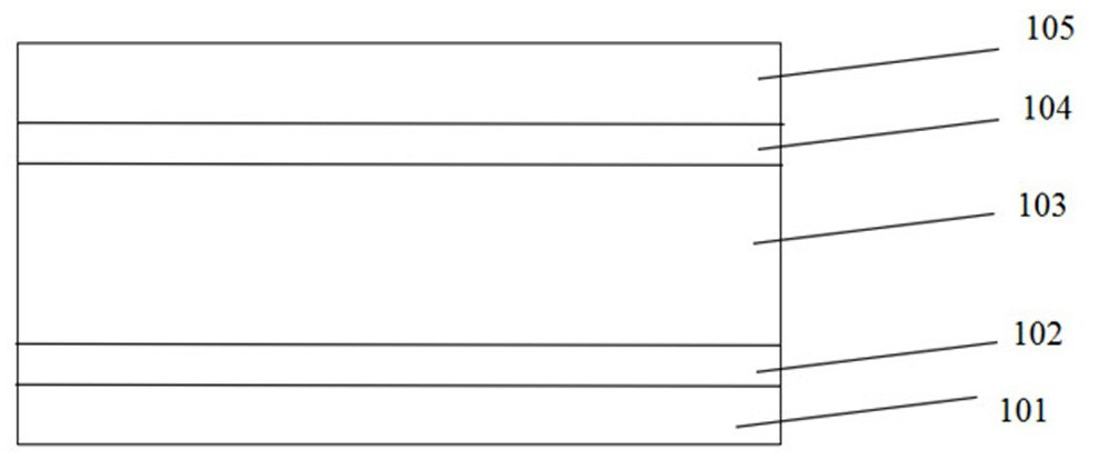
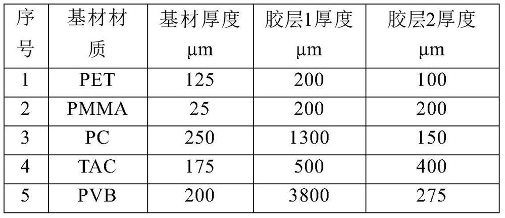
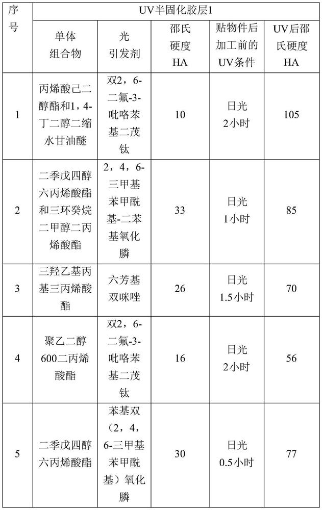
[0028] On one side of the PET substrate layer 101 with a thickness of 125 μm, a UV adhesive layer A with a thickness of 200 μm is coated. The adhesive layer A is composed of hexanediol acrylate and 1,4-butanediol diglycidyl ether, and the added content is 0.1% w / w's photoinitiator bis-2,6-difluoro-3-pyrrole phenyl titanocene forms a UV semi-cured adhesive layer A by UV irradiation, with a Shore hardness of 10HA. Then on the UV semi-cured adhesive layer A, a UV adhesive layer B with a thickness of 100 μm is coated. The adhesive layer B is composed of three (2-hydroxyethyl) isocyanurate diacrylate and isocyanate, and the added content is 0.01% w / The photoinitiator of w, 1-hydroxycyclohexyl phenyl ketone, forms UV semi-cured adhesive layer B through heating and subsequent curing, with a viscosity of 870gf / inch. Paste the protective film on the uneven surface of the device to be processed, let the adhesive layer fill the uneven surface of the device to be processed, and use sunl...

Embodiment 2

[0030] On one side of the PMMA substrate layer 101 with a thickness of 25 μm, a UV adhesive layer A with a thickness of 200 μm is coated, and the adhesive layer A is composed of dipentaerythritol hexaacrylate and tricyclodecane dimethanol diacrylate, and adding a content of 0.2% w / w Photoinitiator 2,4,6-trimethylbenzoyl-diphenylphosphine oxide forms UV semi-cured adhesive layer A by UV irradiation, Shore hardness 33HA. Then on the UV semi-cured adhesive layer A, a UV adhesive layer B with a thickness of 200 μm is coated, and the adhesive layer B is composed of tetraglycidyl benzyl ethane, and a photoinitiator benzophenone with a content of 0.02% w / w is added, UV semi-cured adhesive layer B is formed by UV irradiation, with a viscosity of 2100gf / inch. Paste the protective film on the uneven surface of the device with uneven structure on the surface, let the adhesive layer fill the uneven surface of the device to be processed, and use sunlight to irradiate the surface of the pro...

Embodiment 3

[0032] On one side of the transparent PC substrate layer 101 with a thickness of 250 μm, a UV adhesive layer A with a thickness of 1300 μm is coated. The adhesive layer A is composed of trihydroxyethylpropyl triacrylate, and a photoinitiator hexaaryl with a content of 0.4% w / w is added. Based on bisimidazole, UV semi-cured adhesive layer A is formed by UV irradiation, and the Shore hardness is 26HA. Then, on the UV semi-cured adhesive layer A, a UV adhesive layer B with a thickness of 150 μm is coated. The adhesive layer B is composed of polyethylene glycol 200 dimethacrylate, and a photoinitiator diphenylbenzene with a content of 0.03% w / w is added. Ketone, form UV semi-cured adhesive layer B by UV irradiation, viscosity 1600gf / inch. Paste the protective film on the uneven surface of the device with uneven structure on the surface, let the adhesive layer fill the uneven surface of the device to be processed, and use sunlight to irradiate the surface of the protective film for...


PUM

PropertyMeasurementUnit
thicknessaaaaaaaaaa
thicknessaaaaaaaaaa
thicknessaaaaaaaaaa

Abstract

The invention discloses a surface protection film for processing a device with an uneven structure on the surface. The surface protection film is characterized by sequentially comprising a base material layer, an anti-static layer, a UV semi-cured adhesive layer A, a UV semi-cured adhesive layer B and a release film, wherein the UV semi-cured adhesive layer A and the UV semi-cured adhesive layer Bcontain photoinitiators, the photoinitiators in the adhesive layer A and the adhesive layer B are different in type and dosage, the compositions of the UV semi-cured adhesive layer A and the UV semi-cured adhesive layer B are different, the adhesive layer A is colloidal and soft, the adhesive layer B has pressure-sensitive viscosity, the adhesive layer thicknesses of the UV semi-cured adhesive layer A and the UV semi-cured adhesive layer B are different, and under a certain light irradiation condition, the adhesive layer A is completely cured, and the adhesive layer B is still in a semi-curedstate. According to the invention, when mechanical and chemical processing is carried out on the back surface of a to-be-processed device, the protection film is used for protecting the uneven or microstructure surface of the to-be-processed device and preventing the to-be-processed device from being damaged and polluted in the processing process, and after processing is completed, the protectionfilm can be stripped without adhesive residues; and the protection film has the advantages of simple structure and production process, excellent performance and the like.

Description

technical field [0001] The invention relates to a surface protection film for processing devices with uneven structure on the surface, especially a protection film for the surface with uneven microstructure. Background technique [0002] When mechanical and chemical processing is performed on the back of a device with an uneven surface structure, the uneven or microstructured surface is easily damaged and polluted during processing, and a protective film needs to be attached to the uneven or microstructured surface. The protective film is well attached to the uneven surface, and after the processing is completed, the protective film can be peeled off without adhesive residue. [0003] In the prior art, the strength of the protective film is not enough during the processing of the device. When the device is subjected to mechanical operations such as high-intensity grinding, it is easy to cause damage to the concave-convex surface of the device. Contents of the invention ...

Claims


Application Information

Patent Timeline
Patent Type & Authority Applications(China)
IPC IPC(8): C09J7/25C09J7/24C09J7/30C09J4/02
CPCC09J4/00C09J2433/006C09J2467/006C09J2469/006C09J7/24C09J7/25C09J7/255C09J7/30
Inventor 施克炜陈晓东杨明
Owner TAIHU JINZHANG TECH CO LTD
Why Eureka
Try Eureka