Medium-long wave infrared wide-spectrum light absorption material and preparation method thereof

A light-absorbing material and long-wave infrared technology, which is applied in nanotechnology, optics, and optical components for materials and surface science, can solve the problem that the absorption wavelength is difficult to adjust to the mid-to-far infrared band, light-absorbing materials cannot withstand high temperatures, It is difficult to achieve ultra-wideband light absorption and other problems, to achieve the effects of abundant reserves, improved light absorption efficiency, and mature processing technology

Active Publication Date: 2020-11-03
WUHAN UNIV
View PDF3 Cites 1 Cited by
  • Summary
  • Abstract
  • Description
  • Claims
  • Application Information

AI Technical Summary

Problems solved by technology

The problem with the first idea is that the superposition of multi-band resonance modes is difficult to achieve ultra-wide-band light absorption. Due to the limitation of the plasmon resonance wavelength, it is difficult to adjust the absorption wavelength to the mid-to-far infrared band, and light-absorbing materials containing metal nanostructures Can not withstand high temperature, high power light irradiation and other conditions

Method used


Image

  • Medium-long wave infrared wide-spectrum light absorption material and preparation method thereof
  • Medium-long wave infrared wide-spectrum light absorption material and preparation method thereof
  • Medium-long wave infrared wide-spectrum light absorption material and preparation method thereof

Examples


Embodiment Construction

[0034] For a better understanding of the present invention, the following examples are further descriptions of the present invention, but the content of the present invention is not limited to the following examples.

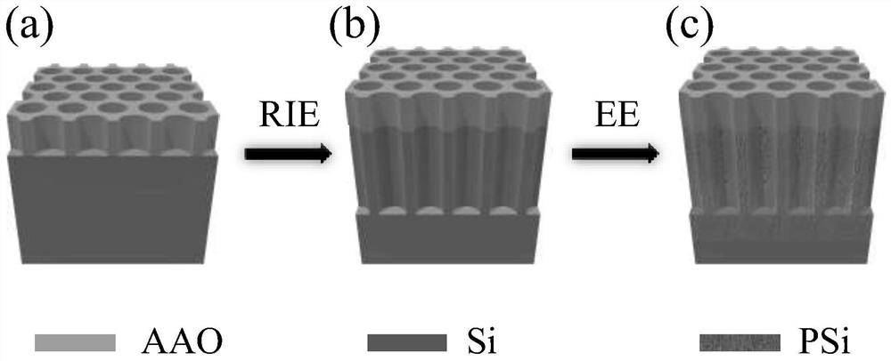
[0035] A method for preparing a medium-long-wave infrared broad-spectrum light-absorbing material, comprising the following steps:

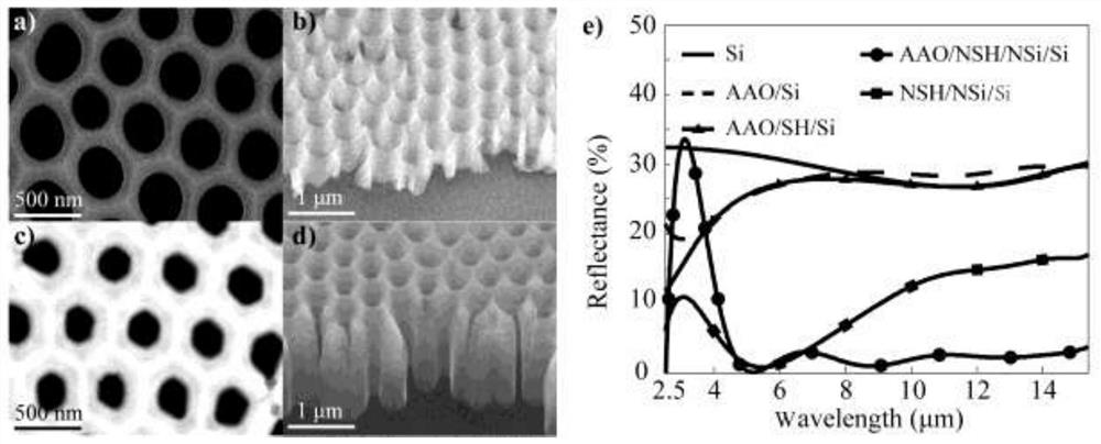
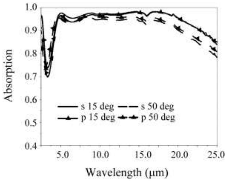
[0036] (1) According to the target absorption spectrum range, the central wavelength is 10 microns, and the dielectric constant Drude model of silicon is used to calculate the bulk plasmon wavelength is not less than 10 microns, the preferred doping concentration is not less than 1.3× 10 18 / cm 3 The heavily doped silicon wafer, by calculating the absorptivity of the selected doping concentration silicon substrate as a function of the absorption depth and wavelength, confirmed that in the 8μm-14μm band, the average absorptivity can be close to 70% at the 9μm absorption depth, the average The reflectivity is 30%.

[0037] (2) The...


PUM

PropertyMeasurementUnit
thicknessaaaaaaaaaa
thicknessaaaaaaaaaa
thicknessaaaaaaaaaa

Abstract

The invention belongs to the field of preparation of inorganic functional materials, and particularly relates to a medium-long-wave infrared wide-spectrum light absorption material and a preparation method thereof, the medium-long-wave infrared wide-spectrum light absorption material is formed by sequentially stacking an alumina pore structure, a silicon pore structure, a silicon nano-pore structure and a silicon substrate; and the silicon nanopore structures are distributed in the silicon hole structures and the silicon substrate. The medium-long-wave infrared wide-spectrum light absorption material is formed by stacking four layers of materials in sequence, a refractive index gradient material is formed, and high-temperature-resistant wide-spectrum light absorption of medium-far infraredbands is achieved through free carrier absorption of a silicon material with the adjustable doping concentration in the medium-long-wave infrared bands. The medium-long wave infrared wide-spectrum light absorption material is large in absorption wavelength range, high in absorption efficiency, small in absorption layer thickness, free of polarization dependence, large in incident angle range andresistant to high temperature.

Description

technical field [0001] The invention belongs to the field of preparation of inorganic functional materials, and in particular relates to a medium-long-wave infrared wide-spectrum light-absorbing material and a preparation method thereof. Background technique [0002] Broad-spectrum light-absorbing materials in the medium and long-wave infrared bands can be used in infrared analog light sources, infrared stealth, infrared photothermal detection, infrared enhanced spectroscopy, waste heat utilization, etc., so they have been valued by research. Among them, broad spectrum, non-polarization dependence, and large incident angle are important performance indicators. In addition, broad-spectrum absorbing materials with high temperature resistance are of great value in aerospace and broad-spectrum infrared thermal light sources. [0003] The structure design of broad-spectrum absorbing materials follows two lines of thought. The first is to enhance the absorption characteristics of...

Claims


Application Information

Patent Timeline
Patent Type & Authority Applications(China)
IPC IPC(8): G02B1/00G02B5/00B82Y30/00
CPCG02B1/00G02B5/003G02B5/008B82Y30/00
Inventor 阮翔宇管志强徐红星
Owner WUHAN UNIV
Why Eureka
Try Eureka