High-brightness LED and preparation method thereof

A technology with high brightness and doping concentration, which is applied in the direction of semiconductor devices, electrical components, circuits, etc., can solve the problems of complicated high-brightness LED preparation process, difficult control of substrate polishing and thinning process, lack of high-brightness LED, etc., to achieve epitaxy The effect of shortening process time, shortening epitaxy process time, and improving luminous efficiency

Pending Publication Date: 2020-11-06
SHANDONG UNIV
View PDF0 Cites 0 Cited by
  • Summary
  • Abstract
  • Description
  • Claims
  • Application Information

AI Technical Summary

Problems solved by technology

Devices prepared by epitaxial growth technology often require a long growth time, or DBR cracks due to stress caused by lattice mismatch; increase the cost of epitaxy and increase the difficulty of the process; through laser lift-off, metal bonding and mechanical polishing process The preparation of optoelectronic devices is not only very difficult to control due to the substrate polishing and thinning process, but also increases the process cost
[0005] Therefore, due to the lack of effective high-brightness LEDs prepared by simple processes so far, the preparation process of high-brightness LEDs is complicated and costly, and it is difficult to control
Therefore, it is necessary to develop a technology with simple growth and preparation process and low cost to realize the preparation of high-brightness LEDs and overcome the bottleneck restricting its application.

Method used


Image

  • High-brightness LED and preparation method thereof
  • High-brightness LED and preparation method thereof
  • High-brightness LED and preparation method thereof

Examples


Embodiment Construction

[0033] The following will clearly and completely describe the technical solutions in the embodiments of the present invention with reference to the drawings in the embodiments of the present invention.

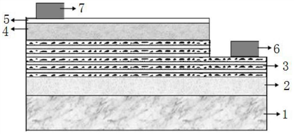
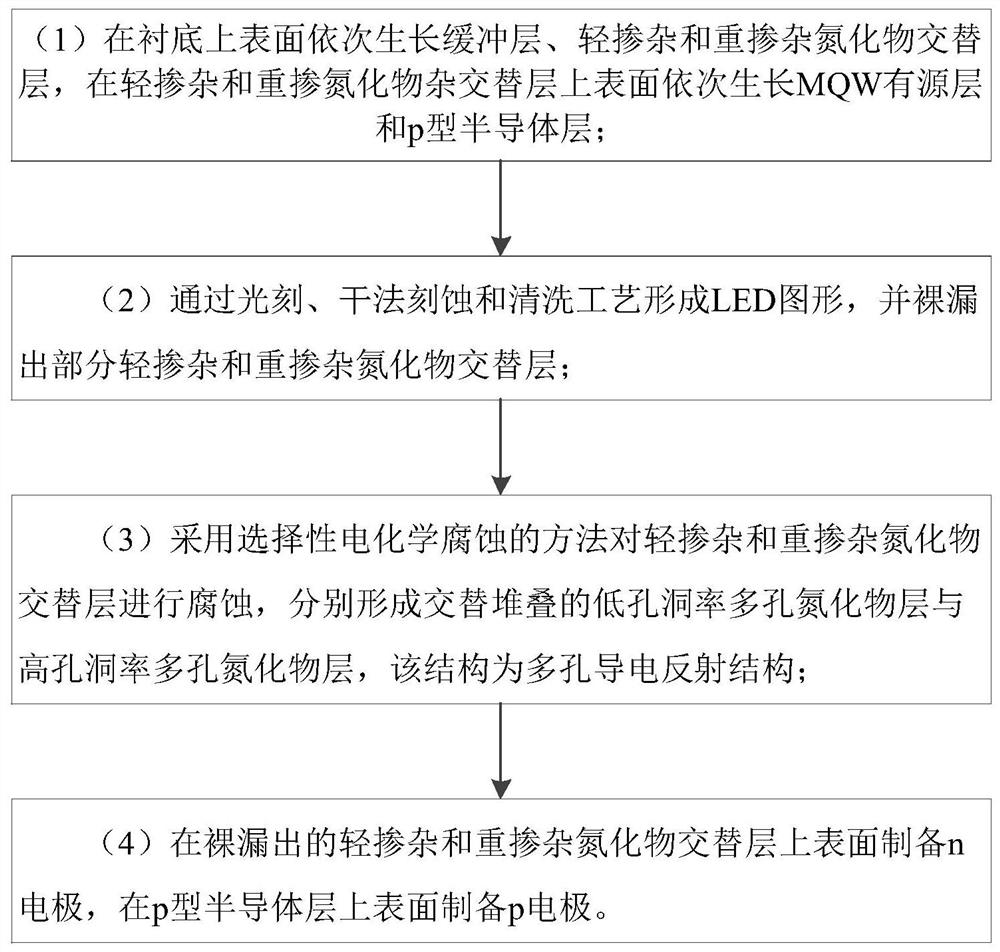
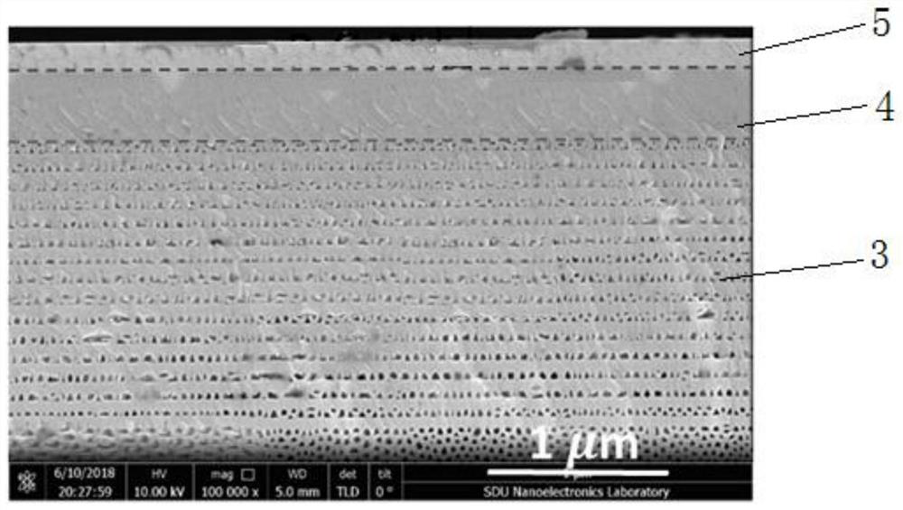
[0034] The invention provides a high brightness LED, such as figure 1 As shown, it includes a substrate 1, on which a buffer layer 2, lightly doped and heavily doped nitride alternating layers 3, MQW active layer 4, and p-type semiconductor layer 5 are sequentially grown, lightly doped and heavily doped An n-electrode 6 is provided on the exposed part of the upper surface of the alternating heteronitride layer 3, and a p-electrode 7 is provided on the p-type semiconductor layer 5; as image 3 As shown, the lightly doped and heavily doped nitride alternating layers 3 are alternately stacked low-porosity porous nitride layers and high-porosity porous nitride layers formed by lightly doped nitride layers and heavily doped nitride layers respectively by electrochemical corrosion. ...


PUM

PropertyMeasurementUnit
Doping concentrationaaaaaaaaaa

Abstract

The invention discloses a high-brightness LED and a preparation method thereof. The high-brightness LED comprises a substrate; a buffer layer, a lightly-doped and heavily-doped nitride alternating layer, an MQW active layer and a p-type semiconductor layer are grown on the substrate in sequence; an n electrode is arranged on the exposed part of the upper surface of the lightly-doped and heavily-doped nitride alternating layer; a p electrode is arranged on the p-type semiconductor layer; the lightly-doped and heavily-doped nitride alternating layer is alternately stacked low-void-ratio porous nitride layers and high-void-ratio porous nitride layers respectively formed by electrochemical corrosion of lightly-doped nitride layers and heavily-doped nitride layers. According to the high-brightness LED and the preparation method thereof disclosed by the invention, the light-emitting efficiency can be improved while the cost is reduced, the repeatability is high, and the practical applicationis facilitated.

Description

technical field [0001] The invention relates to the technical field of LEDs, in particular to a high-brightness LED and a preparation method thereof. Background technique [0002] As the III-nitride wide bandgap semiconductor materials and devices are more widely used in optoelectronics and power electronics fields such as lighting, display, communication and medical treatment, the nitride wide bandgap semiconductor materials and devices as the representative of the third generation of semiconductors have become the most popular in the world. A new generation of fields that are vying to seize. Due to the characteristics of small size, low cost, good monochromaticity and high efficiency, LED has broad application prospects in the fields of lighting, display and optical communication, and has become a research hotspot in the field of optoelectronics, a new generation of electronic information technology. [0003] The main research work of LED focuses on improving its luminous...

Claims


Application Information

Patent Timeline
IPC IPC(8): H01L33/40H01L33/32H01L33/06H01L33/00
CPCH01L33/0075H01L33/06H01L33/325H01L33/405H01L2933/0016
Inventor 张宇韩琳
Owner SHANDONG UNIV
Why Eureka
Try Eureka