Shielding gate power MOSFET with floating electrode and manufacturing method of shielding gate power MOSFET

A floating electrode and manufacturing method technology, applied in semiconductor/solid-state device manufacturing, circuits, electrical components, etc., can solve the problems of large switching loss and large transfer capacitance of the device, and achieve higher breakdown voltage, higher figure of merit, and convenience. effect achieved

Pending Publication Date: 2020-11-10
INST OF MICROELECTRONICS CHINESE ACAD OF SCI
View PDF4 Cites 1 Cited by
  • Summary
  • Abstract
  • Description
  • Claims
  • Application Information

AI Technical Summary

Problems solved by technology

[0005] In view of the above analysis, the present invention aims to provide a shielded gate power MOSFET with a floating electrode and its manufacturing method, in order to solve the problem of large transfer capacitance and large switching loss of the existing device

Method used


Image

  • Shielding gate power MOSFET with floating electrode and manufacturing method of shielding gate power MOSFET
  • Shielding gate power MOSFET with floating electrode and manufacturing method of shielding gate power MOSFET
  • Shielding gate power MOSFET with floating electrode and manufacturing method of shielding gate power MOSFET

Examples


Embodiment 1

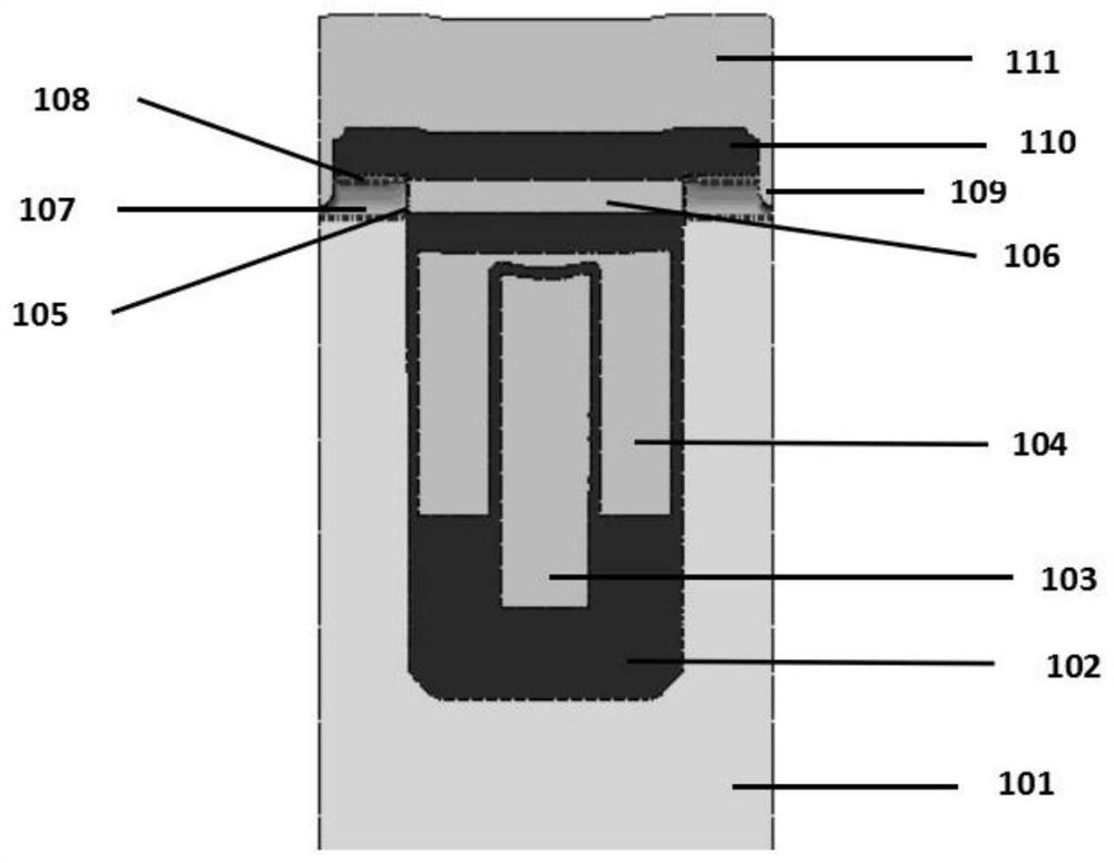
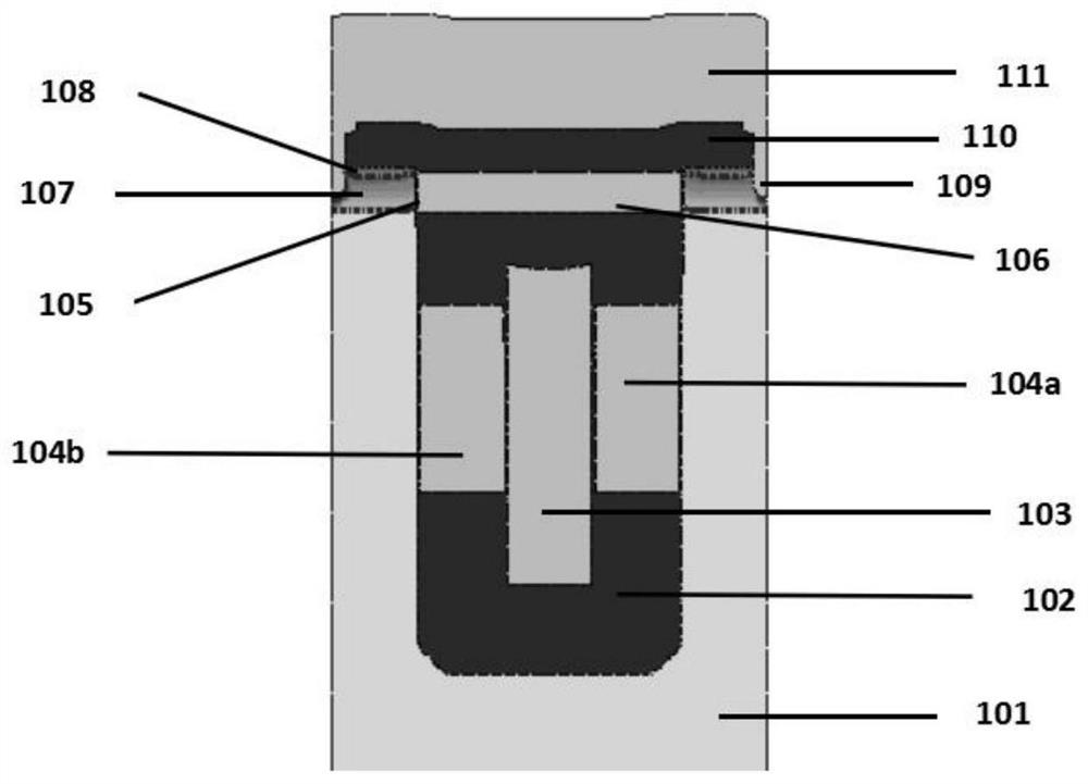
[0052] A specific embodiment of the present invention discloses a shielded gate power MOSFET device with floating electrodes, including a plurality of periodically arranged primary cells, and the gate structure of each primary cell includes a shielding electrode 103, a floating electrode 104 and trench gate electrode 106;

[0053] The shielding electrode 103 is located in the middle of the trench;

[0054] The floating electrodes 104 are located on both sides of the shielding electrode 103 and arranged in the groove;

[0055] The trench gate electrode 106 is located at the top of the trench;

[0056] The shielding electrode 103 , the floating electrode 104 , the trench gate electrode 106 and the inner surface of the trench are isolated from each other by the isolation dielectric layer 102 .

[0057] The electric field distribution in the groove (in the field oxide layer) of the existing shielded gate power MOSFET device is uneven. After setting the floating electrodes 104 on...

Embodiment 2

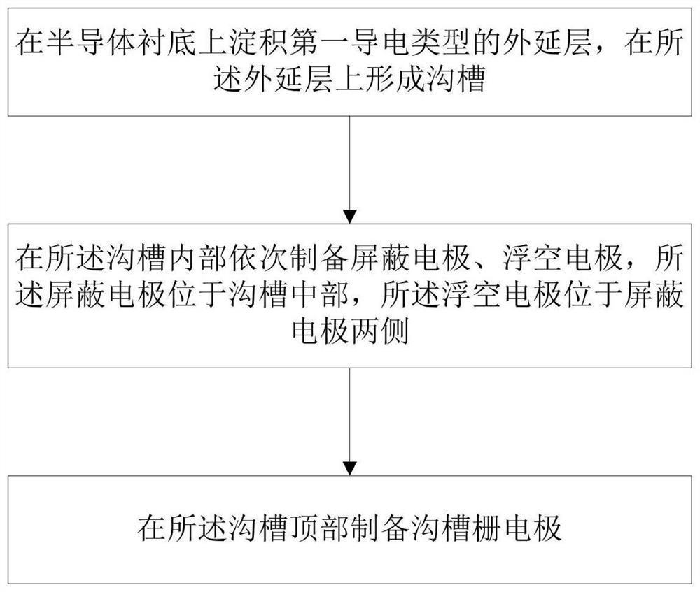
[0074] An embodiment of the present invention provides a method for manufacturing a shielded gate power MOSFET device with a floating electrode, comprising the following steps:

[0075] Step S1, depositing an epitaxial layer of the first conductivity type on the semiconductor substrate, and forming a trench on the epitaxial layer;

[0076] Step S2, sequentially preparing a shielding electrode and a floating electrode inside the trench, the shielding electrode is located in the middle of the trench, and the floating electrodes are located on both sides of the shielding electrode;

[0077] Step S3, preparing a trench gate electrode on the top of the trench.

[0078] By setting floating electrodes on both sides of the shielding electrode, and the floating electrodes are not connected to any electrodes, they are equivalent to equipotential bodies in the electric field, and the potentials on their surfaces are the same, and all electric field lines will be perpendicular to the equi...


PUM

PropertyMeasurementUnit
Thicknessaaaaaaaaaa
Heightaaaaaaaaaa
Widthaaaaaaaaaa

Abstract

The invention relates to a shielding gate power MOSFET device with a floating electrode and a manufacturing method of the shielding gate power MOSFET device, belongs to the technical field of power semiconductor devices, and solves the problems of larger transfer capacitance and smaller breakdown voltage in the prior art. The shielding gate power MOSFET device with the floating electrode comprisesa plurality of primitive cells arranged periodically, and each primitive cell comprises a shielding electrode, the floating electrode and a trench gate electrode. The shielding electrodes are positioned in the middles of the trenches, the floating electrodes are located at the two sides of the shielding electrodes and are arranged in the trenches, the trench gate electrodes are located at the tops of the trenches, and the shielding electrode, the floating electrode, the trench gate electrode and the inner side surface of the trench are isolated from one another through an isolation dielectriclayer, so that the breakdown voltage of the device is improved, and the merit figure of the device is improved.

Description

technical field [0001] The invention relates to the technical field of power semiconductor devices, in particular to a shielded gate power MOSFET with a floating electrode and a manufacturing method thereof. Background technique [0002] With the development of power electronic systems, the power MOSFET (Metal Oxide Semiconductor Field Effect Transistor) device plays an increasingly important role due to its excellent performance, and has become one of the irreplaceable important devices in the field of microelectronics. It is applied to many electronic designs and in application. [0003] MOSFET has the advantages of voltage-controlled turn-on, high input impedance, good thermal stability, and fast switching speed. As early as the 1970s, people began to study the application of MOSFET in power devices. In recent decades, semiconductor manufacturing technology has developed rapidly, and MOSFET manufacturing technology It is becoming more and more mature and the manufacturin...

Claims


Application Information

Patent Timeline
IPC IPC(8): H01L29/78H01L29/40H01L21/336
CPCH01L29/7813H01L29/407H01L29/66734Y02B70/10
Inventor 陈润泽王立新
Owner INST OF MICROELECTRONICS CHINESE ACAD OF SCI
Why Eureka
Try Eureka