
Sn-Zn-In-Ga lead-free solder and preparation method thereof

A lead-free solder and solder technology, used in welding equipment, welding/cutting media/materials, welding media, etc., can solve problems such as the adverse effect of solder wettability, limit the application of Sn-Zn solder, and achieve excellent wettability. , low cost, reducing the effect of influencing factors

Inactive Publication Date: 2020-11-17
HENAN POLYTECHNIC UNIV
View PDF0 Cites 3 Cited by
  • Summary
  • Abstract
  • Description
  • Claims
  • Application Information

AI Technical Summary

Problems solved by technology

However, because Zn is easy to oxidize, it has an adverse effect on the wettability of the solder, which limits the application of Sn-Zn solder

Method used


Image

  • Sn-Zn-In-Ga lead-free solder and preparation method thereof
  • Sn-Zn-In-Ga lead-free solder and preparation method thereof
  • Sn-Zn-In-Ga lead-free solder and preparation method thereof

Examples


Embodiment 1

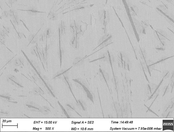
[0026] A Sn-Zn-In-Ga lead-free solder, the lead-free solder is composed of the following components by weight percentage: 7.0% Zn, 0.5% In, 1.0% Ga, the balance is Sn, and unavoidable impurities are also included.

[0027] The preparation method of Sn-Zn-In-Ga lead-free solder alloy is as follows:

[0028] (1) Weigh the raw materials Sn and Zn according to the weight ratio of 1:1 and place them in the crucible of the vacuum induction melting furnace. After vacuuming, fill it with argon for melting. The melting temperature is 550°C~650°C, and the melting time is 30min~40min , a vacuum of 10 -4 Pa, the master alloy Sn-Zn is prepared, the alloy is smelted repeatedly for 3 times, poured into a metal mold after the last remelting, and cooled and solidified in an argon atmosphere;

[0029] (2) Weigh the raw materials Sn and In according to the weight ratio of 1:1 and place them in the crucible of the vacuum induction melting furnace. After vacuuming, fill it with argon for melting....

Embodiment 2

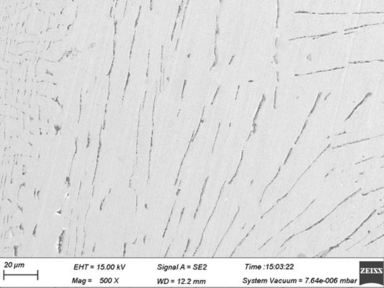
[0033] A Sn-Zn-In-Ga lead-free solder, the lead-free solder is composed of the following components by weight percentage: 7.0% Zn, 1.0% In, 0.5% Ga, the balance is Sn, and unavoidable impurities are also included.

[0034] The preparation method of the lead-free solder alloy of this embodiment is the same as the method of embodiment 1, the only difference is that the weight percentage of the Sn-Zn-In-Ga lead-free solder alloy is added according to the ratio in this embodiment, and will not be repeated here.

Embodiment 3

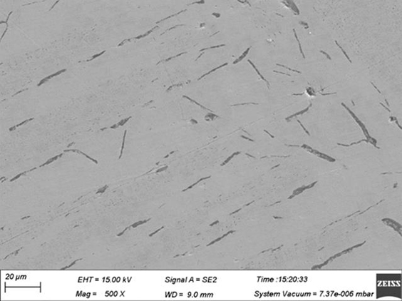
[0036] A Sn-Zn-In-Ga lead-free solder, the lead-free solder is composed of the following components by weight percentage: 7.0% Zn, 0.5% In, 2.0% Ga, the balance is Sn, and unavoidable impurities are also included.

[0037]The preparation method of the lead-free solder alloy in this embodiment is the same as the method in embodiment 1, the only difference is that the weight percentage of the Sn-Zn-In-Ga lead-free solder alloy is added according to the ratio in this embodiment, and will not be repeated here.


PUM


Abstract

The invention provides a lead-free solder for the microelectronics industry and a preparation method thereof. The lead-free solder is prepared from the following components in percentage by weight: 7.0 to 10.0 percent of Zn, 0.05 to 5.0 percent of In, 0.05 to 2.0 percent of Ga, the balance of Sn, and smaller than 0.2 percent of inevitable impurities. The solder contains few components, is low in melting temperature and excellent in wettability, oxidation resistance and mechanical property, can form a good welding joint with various semiconductor materials with different properties in the microelectronics industry, and is suitable for popularization and application.

Description

technical field [0001] The invention relates to a lead-free solder, in particular to a novel Sn-Zn-In-Ga quaternary lead-free solder alloy and a preparation method thereof, belonging to the technical field of soldering materials. Background technique [0002] For a long time, Sn-Pb solder has been widely used in the connection and assembly of electronic products due to its low melting point, low cost and good wettability, and has occupied a dominant position in electronic soldering connection materials. However, in recent years, with people's in-depth understanding of the hazards of lead and its alloys and the improvement of environmental awareness, countries and related organizations around the world have legislated to restrict the application of lead and its alloys in electronic packaging. Therefore, new lead-free solders have been developed. Replacing the traditional Sn-Pb solder has become an urgent task for the electronics industry at home and abroad. [0003] At prese...

Claims


Application Information

Patent Timeline
IPC IPC(8): B23K35/26B23K35/40
CPCB23K35/262B23K35/40
Inventor 徐冬霞曹福磊褚亚东杨毅博任鹏凯和平安
Owner HENAN POLYTECHNIC UNIV
Learn More