Silicon heterojunction solar cell and manufacturing method thereof

A solar cell and silicon heterojunction technology, which is applied in the field of solar cells, can solve problems such as low fill factor, affecting the efficiency of silicon heterojunction solar cells, large series resistance, etc., and achieve the effect of increasing the open circuit voltage and fill factor

Active Publication Date: 2020-11-27
LONGI GREEN ENERGY TECH CO LTD
View PDF5 Cites 2 Cited by
  • Summary
  • Abstract
  • Description
  • Claims
  • Application Information

AI Technical Summary

Problems solved by technology

[0004] However, with the addition of the intrinsic silicon oxide layer, the valence band mismatch between the crystalline silicon substrate and the P-type amorphous silicon layer will be caused.
The mismatch of the valence band will cause a large potential barrier for holes, which will affect the transport of holes, resulting in a large series resistance and a low fill factor of silicon heterojunction solar cells, which will affect the performance of silicon heterojunction solar cells. Improvement in battery efficiency

Method used


Image

  • Silicon heterojunction solar cell and manufacturing method thereof
  • Silicon heterojunction solar cell and manufacturing method thereof
  • Silicon heterojunction solar cell and manufacturing method thereof

Examples


Embodiment 1

[0073] The fabrication method of silicon heterojunction solar cells is as follows:

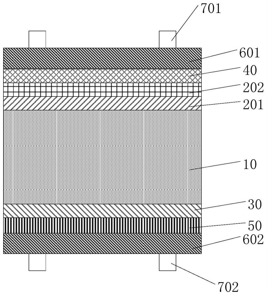
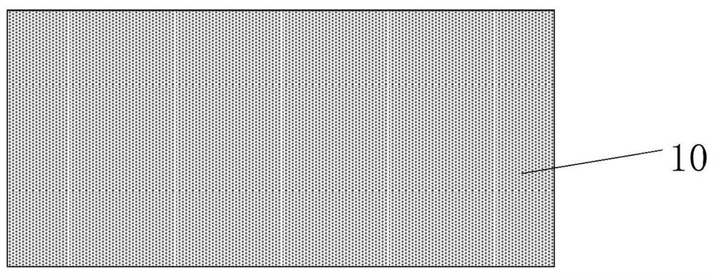
[0074] 1) Surface texturing and cleaning of N-type crystalline silicon wafers (n-c-Si) to form a pyramid structure and remove surface contamination impurities to obtain N-type silicon substrates. Among them, the single crystal silicon substrate used in the N-type crystalline silicon wafer is an N-type double-sided polished Czochralski single crystal silicon wafer with a thickness of 180 μm, a resistivity of 0.3Ω·cm, and a minority carrier lifetime of 1000 μs. Texturing of the silicon wafer was carried out using a mixed solution of 2% NaOH and IPA by mass percentage at a temperature of 83°C. Then, use the RCA standard cleaning method to clean the surface of the silicon wafer to remove surface contamination impurities. Next, remove the surface oxide layer with 1% hydrofluoric acid solution.

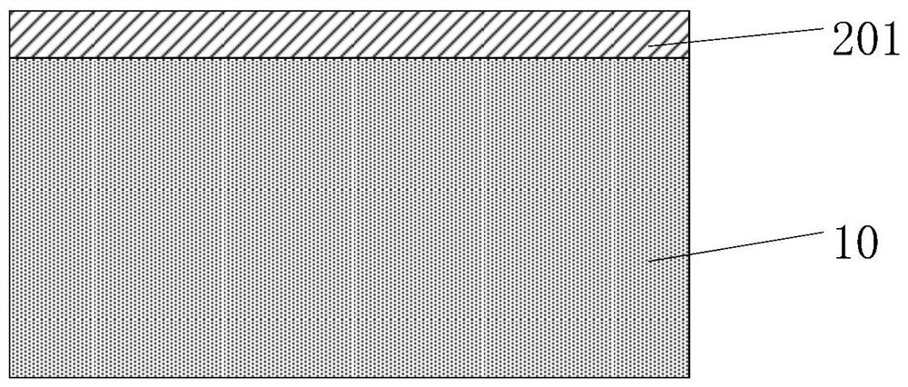
[0075] 2) Deposit a 1nm intrinsic amorphous silicon germanium (i-a-SiGe:H) layer on one side of the N-...

Embodiment 2

[0081] The fabrication method of silicon heterojunction solar cells is as follows:

[0082] 1) For an N-type crystalline silicon wafer (n-c-Si), the surface is textured and cleaned to form a pyramid structure and remove surface contamination impurities to obtain an N-type silicon substrate. Among them, the single crystal silicon substrate used in the N-type crystalline silicon wafer is an N-type double-sided polished Czochralski single crystal silicon wafer with a thickness of 180 μ8, a resistivity of 0.3, and a minority carrier lifetime of 1000 μs. Texturing of the silicon wafer was carried out using a mixed solution of 2% NaOH and IPA by mass percentage at a temperature of 83°C. Then, use the RCA standard cleaning method to clean the surface of the silicon wafer to remove surface contamination impurities. Next, remove the surface oxide layer with 1% by mass hydrofluoric acid solution.

[0083] 2) Deposit a 5nm intrinsic amorphous silicon germanium (i-a-SiGe:H) layer on one...


PUM

PropertyMeasurementUnit
thicknessaaaaaaaaaa
thicknessaaaaaaaaaa
thicknessaaaaaaaaaa

Abstract

The invention discloses a silicon heterojunction solar cell and a manufacturing method thereof, and relates to the technical field of solar cells. The invention aims to inhibit epitaxial growth of a silicon substrate interface by using an intrinsic amorphous silicon germanium layer and improve the passivation effect of the silicon substrate interface by using an intrinsic amorphous silicon layer.The silicon heterojunction solar cell comprises: an N-type silicon substrate; an intrinsic amorphous silicon germanium layer formed on one surface of the N-type silicon substrate; a first intrinsic amorphous silicon layer formed on the intrinsic amorphous silicon germanium layer; and a P-type doped amorphous silicon layer formed on the first intrinsic amorphous silicon layer. The manufacturing method of the silicon heterojunction solar cell is used for manufacturing the silicon heterojunction solar cell.

Description

technical field [0001] The invention relates to the technical field of solar cells, in particular to a silicon heterojunction solar cell and a manufacturing method thereof. Background technique [0002] A silicon heterojunction solar cell is a solar cell in which an intrinsic hydrogenated amorphous silicon layer is added between the P-type amorphous silicon layer and the N-type amorphous silicon layer and the crystalline silicon substrate. The intrinsic amorphous silicon layer is used for Passivation of doped silicon substrates. However, the intrinsic amorphous silicon layer deposited on the crystalline silicon substrate is prone to epitaxial growth, which affects the passivation effect, resulting in a low open circuit voltage, which in turn leads to low efficiency of silicon heterojunction solar cells. And because the epitaxial layer formed on the side of the silicon substrate facing the P-type amorphous silicon layer is within the built-in electric field, the epitaxial la...

Claims


Application Information

Patent Timeline
Patent Type & Authority Applications(China)
IPC IPC(8): H01L31/0747H01L31/0216H01L31/0376H01L31/20
CPCH01L31/0747H01L31/03765H01L31/02167H01L31/204Y02E10/548Y02P70/50
Inventor 徐琛
Owner LONGI GREEN ENERGY TECH CO LTD
Why Eureka
Try Eureka