A method for fabricating upright AU nanocones with high adhesion to substrate surfaces

A substrate surface, high-adhesion technology, applied in the direction of final product manufacturing, sustainable manufacturing/processing, instruments, etc., can solve the problems that cannot be used to improve the adhesion between the upright gold nanocone and the substrate, and the low-temperature aging deformation of the gold nanocone Problems such as low temperature, low adhesion between gold nanocone and substrate, etc., to achieve the effect of easy operation, large range and good controllability

Active Publication Date: 2022-03-29
YANTAI NANSHAN UNIV
View PDF14 Cites 0 Cited by
  • Summary
  • Abstract
  • Description
  • Claims
  • Application Information

AI Technical Summary

Problems solved by technology

In addition to the complicated process or huge cost of these methods, the low adhesion of gold nanocones to the substrate is very low due to the lack of an annealing welding process in most methods
It is worth mentioning here that the low-temperature aging deformation temperature of gold nanocones is very low, so general annealing cannot be used to improve the adhesion of upright gold nanocones to the substrate

Method used


Image

  • A method for fabricating upright AU nanocones with high adhesion to substrate surfaces
  • A method for fabricating upright AU nanocones with high adhesion to substrate surfaces
  • A method for fabricating upright AU nanocones with high adhesion to substrate surfaces

Examples


Embodiment Construction

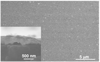
[0022] a. Clean the silicon wafer: Soak the silicon wafer (size 1*1) crystal direction (111) in analytical pure acetone for 3 minutes at room temperature, put the silicon wafer soaked in acetone into an ultrasonic container filled with deionized water , cleaning for 10 min; use CP4A lotion to scratch the surface of the ultrasonically treated silicon wafer until the surface roughness is less than 1 nm; put the scratched silicon wafer into 7% hydrofluoric acid aqueous solution for wet method etching, soaking for 10 min, immersing the silicon wafer after hydrofluoric acid aqueous solution wet etching treatment in an ultrasonic container filled with deionized water, cleaning for 5 min, to obtain a silicon wafer with a clean surface, and using nitrogen gas to clean the silicon wafer Blow dry and store in a desiccator; if figure 1 Shown, 5μm top view and 500nm section view.

[0023] b. Silicon wafer etching: Dip the silicon wafer directly into the etchant for 3 minutes at room temp...


PUM

PropertyMeasurementUnit
surface roughnessaaaaaaaaaa
thicknessaaaaaaaaaa

Abstract

The invention relates to a method for preparing an upright Au nanocone with high adhesion to the surface of a substrate. A large number of nanoscale corrosion holes are etched on the surface of a silicon wafer; Au is evaporated on the surface of a silicon wafer, and further annealed in the etching process. A large-scale Au-Si binary alloy welding point is formed at the Au-Si interface in the hole as the nano-sized clamping end; Au nanocones are prepared on the Au foil and the Si surface by mechanical separation. This structure significantly improves the binding force between the Au nanocones and the substrate, and provides a new technical means for improving the device stability and service life of SERS detectors and solar cells. The design and preparation process of the invention has no special requirements, easy operation and simple equipment requirements, and is especially suitable for commercial large-scale production.

Description

technical field [0001] The invention belongs to the technical field of preparation of microstructure technology, in particular to a method for preparing an upright Au nano cone with high adhesion to a substrate surface. Background technique [0002] Au nanocones have a remarkable light-enhancing effect due to their tips, and have attracted extensive attention in SERS detectors, as well as solar cells. Upright Au nanocones have been prepared by electron beam lithography, nanotransfer printing, nanoimprinting, ultrasonic-assisted interfacial synthesis, and AAO template evaporation coating. In addition to the complicated process or huge cost of these methods, the low adhesion of gold nanocones to the substrate is very low due to the lack of an annealing welding process in most methods. It is worth mentioning here that the low-temperature aging deformation temperature of gold nanocones is very low, so general annealing cannot be used to improve the adhesion of upright gold nano...

Claims


Application Information

Patent Timeline
Patent Type & Authority Patents(China)
IPC IPC(8): H01L31/18H01L31/0236G01N21/65
CPCH01L31/1804H01L31/02363G01N21/658Y02E10/547Y02P70/50
Inventor 李彩琼赵俊凤刘文文赵志国史丹丹史先利董晓燕余鑫祥戴菡
Owner YANTAI NANSHAN UNIV
Why Eureka
Try Eureka