
Connection process of internal binding wire of power module

A technology of power modules and bonding wires, which is applied to semiconductor/solid-state device components, semiconductor devices, electrical components, etc., can solve the problems of reduced power cycle life, complex process, and increased power module loss, etc., to achieve improved power cycle life , increase the contact area, reduce the effect of on-resistance

Active Publication Date: 2020-12-04
WUXI LEAPERS SEMICON CO LTD
View PDF3 Cites 1 Cited by
  • Summary
  • Abstract
  • Description
  • Claims
  • Application Information

AI Technical Summary

Problems solved by technology

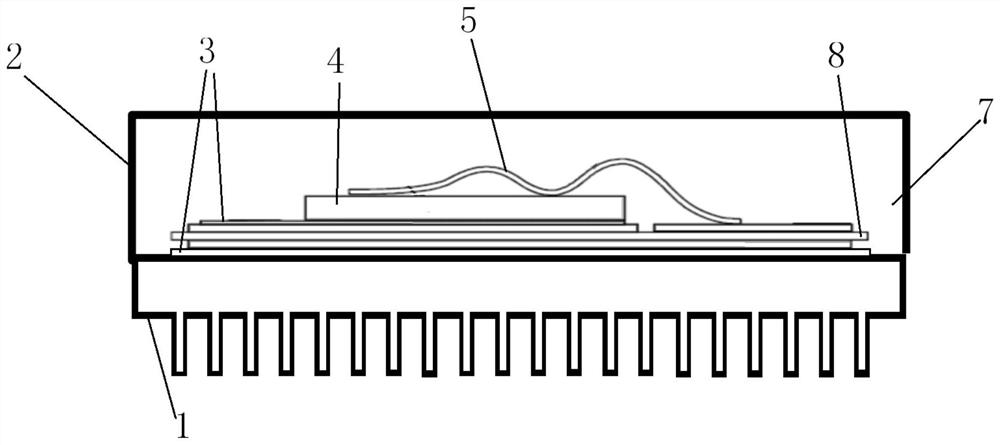
The use of aluminum bonding wires in this way will bring two problems: one is that the number of aluminum bonding wires that can be used is reduced, so that the equivalent conductive cross-sectional area is also reduced, increasing the resistance of the circuit and increasing the loss in the power module. The parasitic inductance of the circuit will also increase; the second is that the power cycle life will also decrease with the reduction of the contact area between the aluminum bonding wire and the chip, because the thermal expansion coefficient of the semiconductor chip is 2 X10 -6 / K to 4X10 -6 / K, aluminum is 23X10 -6 / K, the thermal expansion mismatch of the semiconductor chip during high and low temperature changes will cause mechanical fatigue on the contact surface between the two materials. If the contact area is smaller, the power cycle life will be shorter
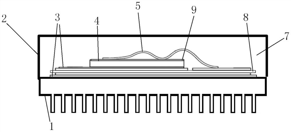
[0004] There are also methods of using copper bonding wires instead of aluminum bonding wires, as shown in the attached figure 2 As shown, but the method of copper bonding wire also has a series of disadvantages. The hardness of copper bonding wire is much greater than that of aluminum bonding wire, and more force is needed to realize the bonding of copper bonding wire and semiconductor chip.
However, semiconductor chips cannot withstand large bonding forces, which often cause chip cracks.
At present, the method to solve this problem is to connect a layer of copper foil layer of tens of microns to 200 microns on the chip to absorb the force when the copper bonding wire is bonded to the surface of the chip, but this method (copper plating or sintered copper foil layer to chip surface) complex and costly
In addition, no matter the aluminum bonding wire or the copper bonding wire, because the general diameter is below 500um, the conductivity has its limit.

Method used


Image

  • Connection process of internal binding wire of power module
  • Connection process of internal binding wire of power module
  • Connection process of internal binding wire of power module

Examples


Embodiment 1

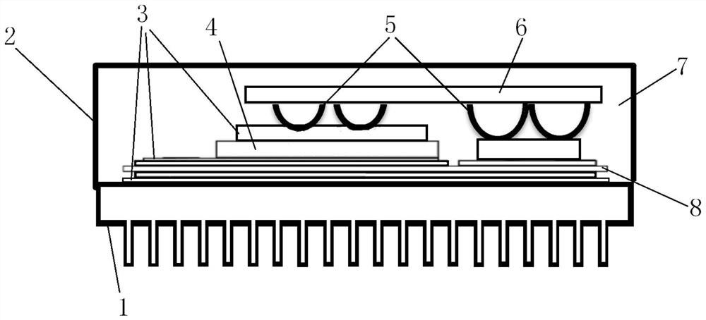
[0023] as attached image 3 As shown, an embodiment of the present invention provides a connection process for bonding wires inside a power module, and the connection process includes the following steps:

[0024] Connect the copper bonding wire with a diameter of 300um to a 1.0mm thick copper plate by ultrasonic bonding, and then connect the copper bonding wire to the semiconductor chip 4 and the power module that have been connected to the insulating heat dissipation material by welding on the electrodes. The shape of the copper bonding wire is arc.

Embodiment 2

[0026] as attached image 3 As shown, an embodiment of the present invention provides a connection process for bonding wires inside a power module, and the connection process includes the following steps:

[0027] Connect the copper bonding wire with a diameter of 500um to a 2mm thick copper plate by ultrasonic bonding, and then connect the copper bonding wire to the semiconductor chip 4 that has been connected to the insulating heat dissipation material and the power module by welding on the electrode. The shape of the copper bonding wire is arc.

Embodiment 3

[0029] as attached image 3 As shown, an embodiment of the present invention provides a connection process for bonding wires inside a power module, and the connection process includes the following steps:

[0030] Connect the copper bonding wire with a diameter of 200um to a 500um thick copper plate by ultrasonic bonding, and then connect the copper bonding wire to the semiconductor chip 4 that has been connected to the insulating heat dissipation material and the power module by welding on the electrode. The shape of the copper bonding wire is arc.

[0031] Specifically, the power modules described in Embodiments 1 to 3 also include a metal base plate 1, a housing 2, a solder layer 3, insulation and heat dissipation materials, silica gel 7, and a double-sided copper-clad ceramic substrate 8 (DBC). The metal bottom plate 1 and the double-sided copper-clad ceramic substrate 8 are connected by welding. The solder layer 3 is soldered with solder paste or tin sheet. The metal bo...


PUM

PropertyMeasurementUnit
Diameteraaaaaaaaaa
Thicknessaaaaaaaaaa

Abstract

The invention is suitable for the technical field of power semiconductor module packaging, and provides a power module internal binding wire connection process, which comprises the following steps ofconnecting a copper binding wire to a metal plate in a bonding mode, and then connecting the copper binding wire to a chip and an electrode of a power module in a welding or sintering mode. Compared with an existing mode that a chip and DBC are connected directly through an aluminum binding wire, the method of the invention has the advantages that the thermal expansion coefficient of a metal plateis close to that of a semiconductor chip, so that the power cycle life is greatly prolonged; compared with an existing mode that a chip and DBC are connected directly through a copper binding wire, the method of the invention has the advantages that the surface of a chip does not need to be connected with a thick copper foil layer, so that the process is simple, and the cost is low; and comparedwith the two modes, the method of the invention has the advantages that the contact area with the surface of the chip is increased, most of the circuit passes through a thick metal plate, the on-resistance is greatly reduced, and the parasitic inductance is also reduced.

Description

technical field [0001] The invention belongs to the technical field of packaging of power semiconductor modules, and in particular relates to a connection process of bonding wires inside a power module. Background technique [0002] In the application of power supply and power electronic converter, power semiconductor (IGBT, MOSFET, SiC, GaN, etc.) devices are widely used, and the package form of module is generally used in the case of high power. The packaging form that is widely used now: the power module is mainly composed of a metal base plate, a solder layer, DBC (double-sided copper-clad ceramic substrate), AMB (foil brazed copper-clad ceramic substrate), insulating and heat-dissipating resin film or other insulating and heat-dissipating materials, Bonding wire, casing and silica gel; after the power semiconductor chip is fixed to the insulating and heat-dissipating material by welding, it is electrically connected through an aluminum bonding wire, and then the DBC o...

Claims


Application Information

Patent Timeline
IPC IPC(8): H01L21/60H01L21/607H01L23/49
CPCH01L24/85H01L24/48H01L2224/85205H01L2224/85801H01L2224/8584H01L2224/48091H01L2224/32225H01L2224/73265H01L2224/48227H01L2224/40225H01L2224/4846H01L2224/45015H01L2224/45124H01L2224/45147H01L2224/73221H01L2924/00012H01L2924/2076H01L2924/00014H01L2924/00
Inventor 梁小广
Owner WUXI LEAPERS SEMICON CO LTD
Learn More