Preparation method of silicon carbide power diode device

A technology of power diodes and silicon carbide, applied in semiconductor/solid-state device manufacturing, semiconductor devices, electrical components, etc., can solve problems such as device reliability impact, device electrical failure, ohmic metal corrosion, etc., to improve yield and reduce Conduction voltage drop, the effect of ensuring integrity

Active Publication Date: 2020-12-04
XIAMEN SANAN INTEGRATED CIRCUIT
View PDF4 Cites 3 Cited by
  • Summary
  • Abstract
  • Description
  • Claims
  • Application Information

AI Technical Summary

Problems solved by technology

The BOE (Buffered Oxide Etch) solution used in wet etching, that is, the buffered oxide etching solution, will cause corrosion to the front ohmic metal, and the metal particles will be contaminated with the BOE solution in various positions of the device, including the active area or The terminal area forms a leakage channel, causing electrical failure of the device, and even affecting the reliability of the device

Method used


Image

  • Preparation method of silicon carbide power diode device
  • Preparation method of silicon carbide power diode device
  • Preparation method of silicon carbide power diode device

Examples


Embodiment Construction

[0046] The present invention will be further described in detail below in conjunction with the accompanying drawings and embodiments.

[0047] In order to solve the problem that the surface of the device is easily contaminated by metal particles in the preparation method of the prior art, a method for preparing a silicon carbide power diode device is provided, which can reduce the reliability risk caused by the contamination of metal particles and avoid the generation of metal particles The problem of contaminating devices can greatly improve the yield rate of device manufacturing.

[0048] The preparation method of silicon carbide power diode device described in the present invention, comprises the following steps:

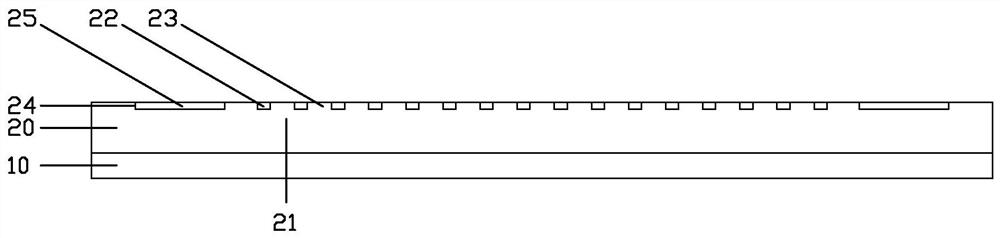
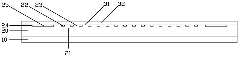
[0049] 1) growing a SiC epitaxial layer 20 with an N-type active region 21 on the first surface of the SiC substrate 10, such as figure 1 shown. Specifically, the RCA cleaning process is performed on the SiC substrate 10, the crystal type of the SiC substrate 1...


PUM


Abstract

The invention relates to a preparation method of a silicon carbide power diode device. The preparation method comprises the following steps: growing a SiC epitaxial layer with an N type active regionon a first surface of a SiC substrate; depositing a first barrier layer on the surface of the SiC epitaxial layer, opening an injection window in the N type active region through etching, and performing ion injection in the injection window of the N type active region; through high-temperature activation, forming P type regions arranged at intervals in the N type active region; and covering a first metal layer forming ohmic contact with the P type region with a second metal layer, so that the first metal layer is prevented from being corroded by a BOE solution in the process of removing the second barrier layer through wet etching, the integrity of the first metal layer is greatly guaranteed, the problem that metal particles contaminate a device is avoided, the reliability risk caused by metal particle contamination is reduced, and the device manufacturing yield is greatly improved.

Description

technical field [0001] The invention relates to the technical field of semiconductor devices, in particular to a method for preparing a silicon carbide power diode device. Background technique [0002] Compared with traditional Si-based devices, SiC devices have the characteristics of faster operating frequency, lower operating loss, and higher operating temperature. As a representative device of SiC power devices, SiC diodes are widely used in power supplies, new energy vehicles and other fields. [0003] Due to the difference in the characteristics of SiC material and Si material, the process difference in its device preparation is caused. For example, if the temperature of the high-temperature activation process of SiC devices reaches above 1600°C, it is necessary to make a protective layer on the front and back of the wafer to prevent the precipitation of carbon particles and affect the interface state of the device. [0004] In the preparation of SiC MPS (Merged PiN Sc...

Claims


Application Information

Patent Timeline
IPC IPC(8): H01L29/16H01L29/06H01L29/868H01L29/872H01L21/329
CPCH01L29/1608H01L29/0684H01L29/872H01L29/868H01L29/6606
Inventor 陶永洪蔡文必彭志高
Owner XIAMEN SANAN INTEGRATED CIRCUIT
Why Eureka
Try Eureka