High-precision ultrathin PCB preparation method

A high-precision, ultra-thin technology, which is applied in the fields of printed circuit manufacturing, multi-layer circuit manufacturing, and printed circuit precursor manufacturing. It can solve the problems of the overall thickness of copper lines and poor heat dissipation performance, and achieve high mechanical strength. , Anti-oxidation, strong ability to resist breakdown voltage

Active Publication Date: 2020-12-22
光臻精密制造(苏州)有限公司
View PDF4 Cites 0 Cited by
  • Summary
  • Abstract
  • Description
  • Claims
  • Application Information

AI Technical Summary

Problems solved by technology

[0004] Therefore, the technical problem to be solved by the present invention is to overcome the defects that direct copper plating in the existing printed circuit board process is likely to cause copper lines to w...

Method used


Image

  • High-precision ultrathin PCB preparation method
  • High-precision ultrathin PCB preparation method
  • High-precision ultrathin PCB preparation method

Examples


Embodiment 1

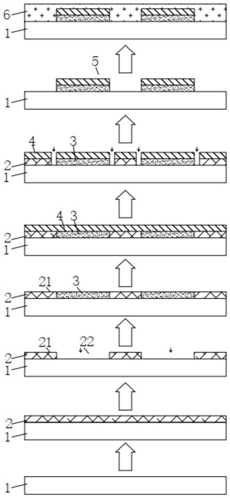
[0052] This embodiment provides a high-precision ultra-thin PCB preparation method, such as figure 1 shown, including the following steps:

[0053] (1) Provide substrate

[0054] The base material 1 is cut according to the preset size, and the purpose is to reduce waste as much as possible; the material of the base material 1 is a copper-free core board with at least one of FR-4, PTFE, PI, and ceramics as the medium. In this embodiment, the substrate 1 adopts a copper-free core board with PTFE as the medium, and the thickness is controlled within the range of 20-25 μm.

[0055] In order to facilitate subsequent processing, the base material 1 needs to be pretreated, such as roughening, cleaning, drying, and punching.

[0056] Wherein, the roughening treatment process is: soaking in lye at 65-70° C. for 40-50 minutes, and the lye includes the following raw materials in parts by weight: 8-10 parts of sodium methoxide and 4-5 parts of potassium tert-butoxide. The purpose is to...


PUM

PropertyMeasurementUnit
Thicknessaaaaaaaaaa
Thicknessaaaaaaaaaa
Thicknessaaaaaaaaaa

Abstract

The invention belongs to the technical field of circuit board manufacturing, and particularly relates to a high-precision ultrathin PCB preparation method which comprises the following steps: forminga mask on the surface of a substrate; etching the mask according to a pre-designed printed circuit trend to form a pattern with a concave region and a convex region; injecting a nickel-based metal ionpolyethylene glycol methacrylate resin mixture into the sunken area to form a priming coat; depositing Cu layers on the surface of the priming coat and the convex region; removing the Cu layer located in the convex region and the residual mask; and forming a flat insulating layer to obtain the high-precision ultrathin PCB. Polyethylene glycol methacrylate resin is added to form a mixture with nickel-based metal ions, so that the bonding strength of a priming coat and a base material is improved, the Cu layer is deposited on the priming coat, the bonding strength of the Cu layer and the priming coat is enhanced, the bonding strength of a copper circuit and the base material is finally realized, and the problem of short circuit or open circuit caused by tilting of the copper circuit does not exist. High-quality transmission of PCB signals is ensured.

Description

technical field [0001] The invention belongs to the technical field of circuit board manufacturing, and in particular relates to a method for preparing a high-precision ultra-thin PCB. Background technique [0002] In recent years, with the rapid development of the electronic information technology industry, the structure of electronic products has become more and more complex, and the functions have become more and more comprehensive, which will promote the development of printed circuit boards (PCBs) that constitute electronic products in the following two directions: (1 ) There are more and more functional components integrated on electronic products, but the overall size is getting smaller and smaller, which will promote the continuous development of PCBs in the direction of high precision and high integration, requiring PCBs to gradually change from conventional single-layer design to multi-layer design or even High-density interconnection structure design; (2) Electron...

Claims


Application Information

Patent Timeline
IPC IPC(8): H05K3/38H05K1/02H05K3/02H05K3/46
CPCH05K3/386H05K1/0271H05K1/0209H05K3/022H05K3/4644H05K3/4673
Inventor 郝家胜
Owner 光臻精密制造(苏州)有限公司
Why Eureka
Try Eureka