Shield gate MOSFET device with uniformly doped channel and processing technology

A uniform doping and shielding gate technology, which is applied in semiconductor devices, semiconductor/solid-state device manufacturing, electrical components, etc., can solve the problems of unfavorable device threshold stability, narrowing of P-region depletion region, uneven concentration distribution, etc., to achieve The effect of reducing the risk of punch-through, stabilizing the threshold voltage, and good doping concentration

Pending Publication Date: 2021-01-01
VANGUARD SEMICON CORP
View PDF0 Cites 5 Cited by
  • Summary
  • Abstract
  • Description
  • Claims
  • Application Information

AI Technical Summary

Problems solved by technology

However, compared with traditional MOSFETs, the selection of the epitaxial wafer in the drift region of the shielded gate MOSFET device makes its concentration close to the doping concentration of the P-type (N-type) body region, resulting in narrowing of the depletion region of the P region, and the drain in low-voltage applications. The current increases, and there is a risk of punch-through during the withstand voltage process
In addition, in terms of processing technology, most of the preparation methods for P-type (N-type) body regions are ion implantation and high temperature pushing junction. The obvious disadvantage of this preparation method is that the concentration of the body region formed by diffusion changes with the increase of junction depth. Larger, especially in the case of high concentration in the drift region, its compensation effect on the concentration of the body region is particularly obvious, making the concentration distribution uneven when the channel is finally formed, and the process deviation is large, which is not conducive to the threshold stability of the device

Method used


Image

  • Shield gate MOSFET device with uniformly doped channel and processing technology
  • Shield gate MOSFET device with uniformly doped channel and processing technology
  • Shield gate MOSFET device with uniformly doped channel and processing technology

Examples


Embodiment Construction

[0034] Embodiments of the present invention are described below through specific examples, and those skilled in the art can easily understand other advantages and effects of the present invention from the content described in this specification. The present invention can also be implemented or applied through other different specific implementation modes, and various modifications or changes can be made to the details in this specification based on different viewpoints and applications without departing from the spirit of the present invention.

[0035] Below in conjunction with accompanying drawing, describe technical scheme of the present invention in detail:

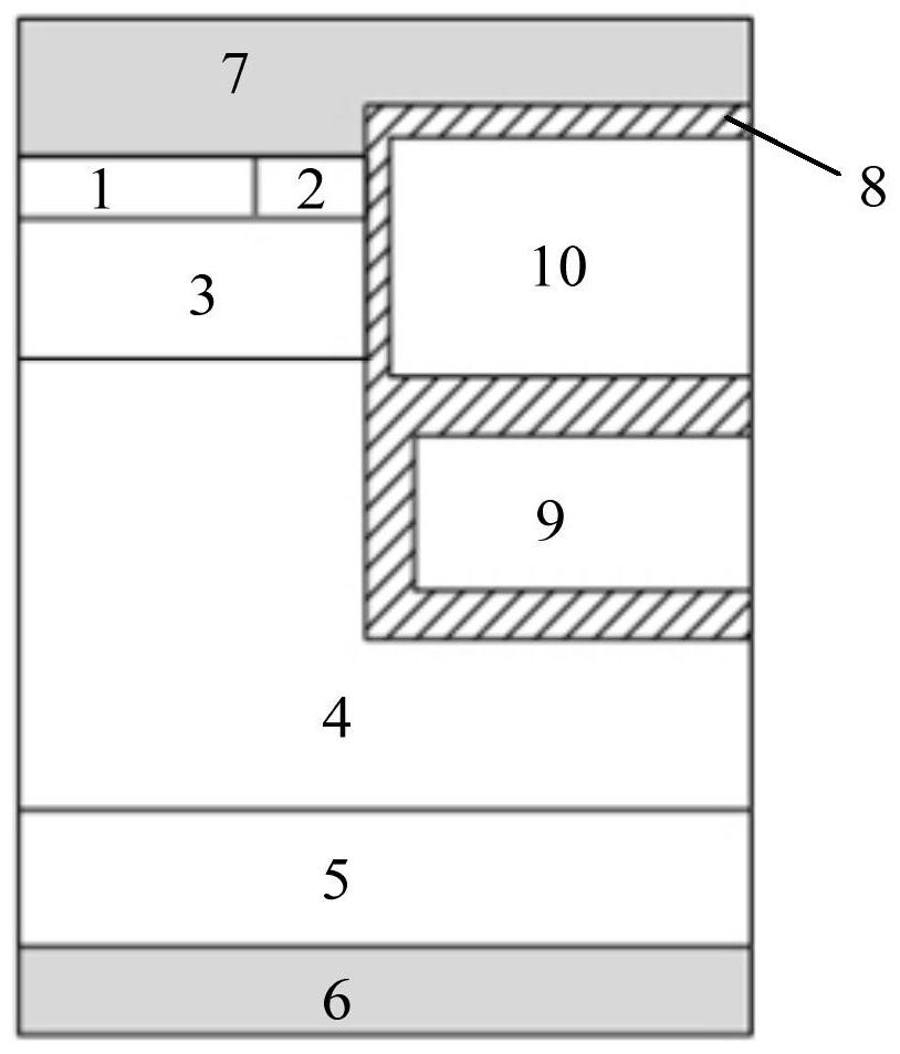
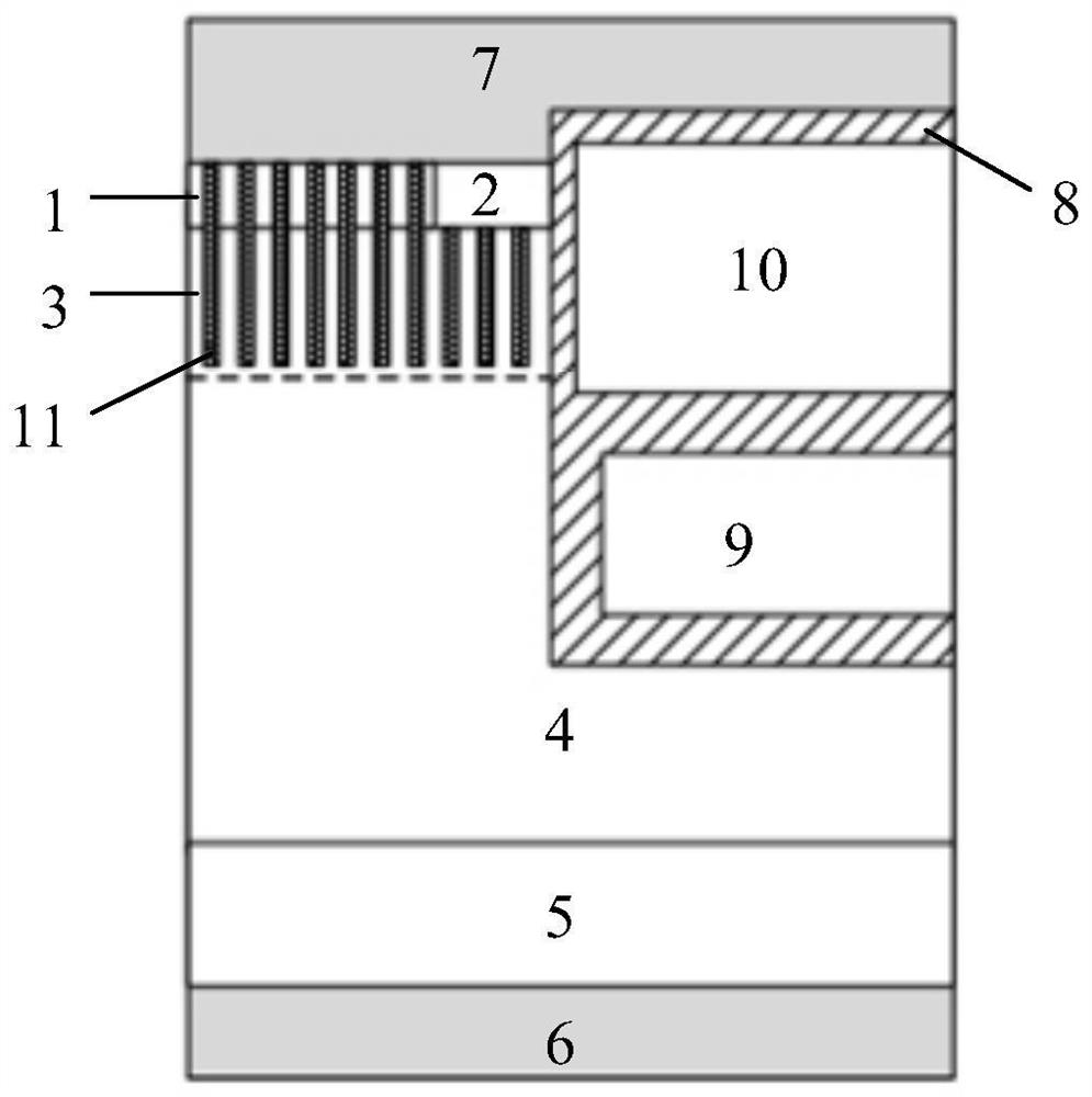
[0036] In a specific embodiment, the semiconductor of the first conductivity type is a P-type semiconductor, and the semiconductor of the second conductivity type is an N-type semiconductor. In another specific embodiment, the semiconductor of the first conductivity type is an N-type semiconductor, and the semiconduct...


PUM


Abstract

The invention discloses a shield gate MOSFET device with a uniformly doped channel and a processing technology, which are characterized in that on the basis of the existing shield gate MOSFET device,a heavily doped first conductive type polycrystalline silicon column region is formed in a groove etching heavily doped polycrystalline silicon filling mode, and then a first conductive type body region is formed in a rapid thermal annealing mode; by optimizing the doping concentration of the first conductive type body region, a mutation junction is formed between the first conductive type body region and the drift region, so that the threshold consistency of the device is improved, meanwhile, the problem that the first conductive type body region is excessively compensated by the drift regionis solved, the doping concentration of the body region is improved, and the possibility that a parasitic triode of the device is turned on is reduced; reliability of the device is improved.

Description

technical field [0001] The invention relates to the technical field of power semiconductor devices, in particular to a shielded gate MOSFET device with a uniformly doped channel and a processing technology. Background technique [0002] As the core of electric energy conversion and power application, power semiconductor devices are the key technologies in the fields of industrial electronics and consumer electronics. As a type of device with the largest market share of power semiconductor discrete devices, MOSFETs have excellent characteristics, especially in applications in the low-voltage field. Compared with bipolar devices, the unipolar characteristics of MOS devices have higher input impedance, faster switching speed, and easier Drive, low transient power consumption and other advantages. In order to improve the withstand voltage of the device, the power MOSFET device has experienced continuous development from the lateral structure to the vertical structure, from the ...

Claims


Application Information

Patent Timeline
Patent Type & Authority Applications(China)
IPC IPC(8): H01L29/78H01L29/06H01L29/10H01L21/336
CPCH01L29/0619H01L29/1037H01L29/66734H01L29/7813
Inventor 李泽宏赵一尚胡汶金林泳浩李伟聪
Owner VANGUARD SEMICON CORP
Why Eureka
Try Eureka