Manufacturing process of bulk acoustic wave resonator and bulk acoustic wave resonator

A bulk acoustic wave resonator and manufacturing process technology, applied in electrical components, impedance networks, etc., can solve the problems of increasing filter size, affecting device performance, affecting resonator frequency response, etc., to suppress parasitic oscillation, simplify wiring, improve effect on device performance

Active Publication Date: 2021-01-08
HANGZHOU XINGHE TECH CO LTD
View PDF23 Cites 1 Cited by
  • Summary
  • Abstract
  • Description
  • Claims
  • Application Information

AI Technical Summary

Problems solved by technology

The bottom electrode spans the upper part of the cavity to ensure the mechanical stability of the resonator. When the electrode is connected to other resonators or the signal source is introduced, it needs to be extended to a sufficient length to ensure the normal transmission of electrical signals. At this time, the edge extending outside the effective working area The top electrode and the bottom electrode form an electric field under the external signal source to excite the piezoelectric layer between them to generate mechanical waves and cause parasitic oscillations, which directly affect the frequency response of the resonator, and further cause waveform instability in the passband of the filter and other deterioration of device performance. Therefore, the structural design of the resonator becomes a difficult problem
[0004] The resonator structure in the prior art generally isolates the interaction of the upper and lower electrodes through the Air gap at the boundary of the cavity to suppress the parasitic oscillation and resonance interference outside the effective area. The Air gap is made by releasing its internal sacrificial layer, and it is necessary to ensure that the piezoelectric layer The mechanical stability of the top electrode of the suspended part above, the top electrode film is stacked on the piezoelectric layer, considering the mechanical stability of the top electrode, especially in the high frequency band, the thickness of the electrode and the piezoelectric layer becomes very thin (100nm), Stress control and mechanical stability will become very challenging
Or a staggered electrode structure is used to avoid the parasitic interference between the upper and lower electrodes. The staggered simple electrode structure is attached to the Air gap structure on the substrate. The formation of the above-mentioned Air gap requires a complicated process, and the sides of the cavity are very steep. Growth with piezoelectric layers on steep cavity sides can create severe stress and / or film defects that can affect device performance
Or use the mass load on the top to form a sudden change in acoustic impedance to suppress the energy taken away by the shear wave and increase the Q value, but the piezoelectric layer on the edge of the cavity will replicate the lattice defects and micropores brought about by the etching process of the bottom electrode. Affect device performance
Or by making a groove on the piezoelectric layer to form a region with a sudden change in acoustic impedance to suppress the energy taken away by the shear wave and increase the Q value. The groove is made by etching a recess on the piezoelectric layer. The etching process will cause the bottom of the groove and the The lattice defects and micro-holes of the piezoelectric layer on the side wall, and even the quality of the piezoelectric layer film around the groove will also be affected to varying degrees. The stress distribution of the original grown ALN ​​film is destroyed, and the stress change is difficult to control and deteriorates. The performance of the resonator, on the other hand, reduces the area of ​​the resonant region in the upper part of the cavity, which increases the size of the filter to a certain extent
There are also some other staggered electrode structures. Although the parasitic interference between the upper and lower electrodes is avoided, it is easy to cause energy leakage, which makes its Q value very low.

Method used


Image

  • Manufacturing process of bulk acoustic wave resonator and bulk acoustic wave resonator
  • Manufacturing process of bulk acoustic wave resonator and bulk acoustic wave resonator
  • Manufacturing process of bulk acoustic wave resonator and bulk acoustic wave resonator

Examples


Embodiment Construction

[0037]The application will be further described in detail below in conjunction with the accompanying drawings and embodiments. It should be understood that the specific embodiments described here are only used to explain related inventions, rather than to limit the invention. It should also be noted that, for the convenience of description, only the parts related to the related invention are shown in the drawings.

[0038] It should be noted that, in the case of no conflict, the embodiments in the present application and the features in the embodiments can be combined with each other. The present application will be described in detail below with reference to the accompanying drawings and embodiments.

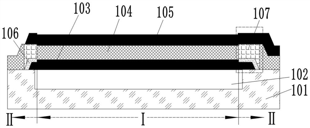
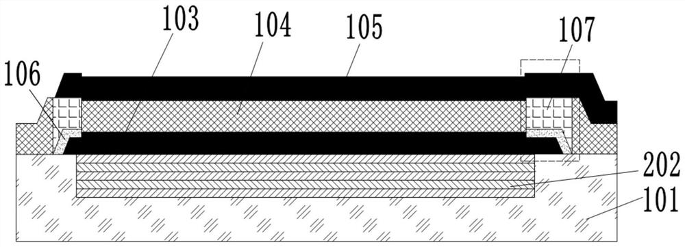
[0039] figure 1 A schematic cross-sectional view of a bulk acoustic wave resonator according to an embodiment of the present invention is shown, as figure 1 As shown, the BAW resonator includes a substrate 101 , an acoustic mirror 102 , a bottom electrode 103 , a piezoelectr...


PUM


Abstract

The invention discloses a manufacturing process of a bulk acoustic wave resonator, which comprises the following steps: manufacturing an acoustic reflector on a substrate, and manufacturing a bottom electrode layer for covering the acoustic reflector on the substrate; carrying out chemical treatment on the peripheral part of the bottom electrode layer to form a modified layer, wherein the modifiedlayer surrounds the bottom electrode layer; manufacturing a piezoelectric layer on the bottom electrode layer; and manufacturing a top electrode layer on the piezoelectric layer. Also disclosed is abulk acoustic wave resonator including a substrate, an acoustic mirror formed on the substrate, and a bottom electrode layer, a piezoelectric layer, and a top electrode layer sequentially formed on the substrate having the acoustic mirror, wherein a portion, adjacent to an edge of the acoustic mirror, of the bottom electrode layer is chemically treated to form the modified layer. By means of the formation of the modified layer, the electric field intensity between the outer electrodes in the effective working area is weakened or eliminated, the electrodes cannot excite the piezoelectric layerbetween the electrodes to generate mechanical waves, parasitic oscillation of the resonator is restrained, and meanwhile wiring of the top electrode is greatly simplified.

Description

technical field [0001] The present application relates to the field of communication devices, and mainly relates to a manufacturing process of a bulk acoustic wave resonator and the bulk acoustic wave resonator. Background technique [0002] With the increasingly crowded electromagnetic spectrum and the increase of frequency bands and functions of wireless communication equipment, the electromagnetic spectrum used by wireless communication has grown rapidly from 500MHz to above 5GHz. Therefore, there is a demand for RF front-end modules with high performance, low cost, low power consumption, and small size. also growing. The filter is one of the RF front-end modules, which can improve the transmitted and received signals, and is mainly composed of multiple resonators connected through a topology network structure. Baw (Bulk Acoustic Wave) is a bulk acoustic wave resonator. The filter composed of it has the advantages of small size, strong integration ability, high quality f...

Claims


Application Information

Patent Timeline
Patent Type & Authority Applications(China)
IPC IPC(8): H03H3/02H03H9/02H03H9/17
CPCH03H3/02H03H9/02125H03H9/0211H03H9/02157H03H9/02H03H9/175H03H9/174H03H2003/025H03H2003/023H03H2003/028H03H2009/02173
Inventor 李林萍盛荆浩江舟
Owner HANGZHOU XINGHE TECH CO LTD
Why Eureka
Try Eureka