Manufacturing method of gallium arsenide-based semiconductor device
A gallium arsenide-based, manufacturing method technology, applied in semiconductor/solid-state device manufacturing, electrical components, circuits, etc., can solve problems such as lower product yield, easy peeling off of silicon nitride protective film, and easy cracks
- Summary
- Abstract
- Description
- Claims
- Application Information
AI Technical Summary
Problems solved by technology
Method used
Image

Examples
Embodiment
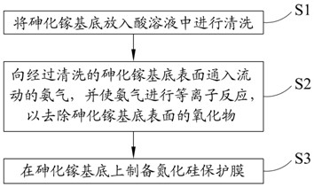
[0033] like figure 1 As shown, the manufacturing method of the gallium arsenide-based semiconductor device provided in this embodiment includes:
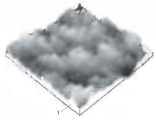
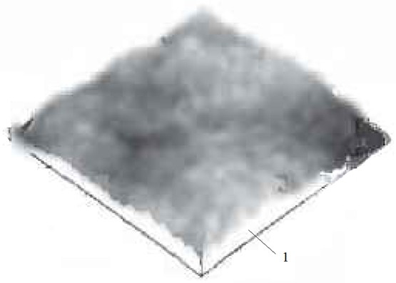
[0034] Step S1: putting the gallium arsenide substrate 1 into an acid solution for cleaning;
[0035] Step S2: Flowing ammonia gas into the surface of the cleaned gallium arsenide substrate 1, and causing the ammonia gas to undergo a plasma reaction, so as to remove oxides on the surface of the gallium arsenide substrate 1;
[0036] Step S3: preparing a silicon nitride protective film on the gallium arsenide substrate 1 .
[0037] In the method for manufacturing a gallium arsenide-based semiconductor device provided in this embodiment, before preparing a silicon nitride protective film on the gallium arsenide substrate 1 cleaned with an acid solution, flow ammonia gas into the surface of the gallium arsenide substrate 1 and make the The ammonia gas undergoes a plasma reaction, and then the oxide on the surface of the gallium arsen...
PUM
 Abstract
Description
Claims
Application Information
 - R&D
- Intellectual Property
- Life Sciences
- Materials
- Tech Scout
- Unparalleled Data Quality
- Higher Quality Content
- 60% Fewer Hallucinations
Browse by: Latest US Patents, China's latest patents, Technical Efficacy Thesaurus, Application Domain, Technology Topic, Popular Technical Reports.
© 2025 PatSnap. All rights reserved.Legal|Privacy policy|Modern Slavery Act Transparency Statement|Sitemap|About US| Contact US: help@patsnap.com