Deep trench MOSFET device structure with low on-resistance

A technology with low on-resistance and device structure, applied in semiconductor devices, electrical components, circuits, etc., can solve problems such as hindering characteristic on-resistance, large proportion of MESA resistance, and reduction

Inactive Publication Date: 2021-01-26
XIAN LONTEN RENEWABLE ENERGY TECH
View PDF2 Cites 2 Cited by
  • Summary
  • Abstract
  • Description
  • Claims
  • Application Information

AI Technical Summary

Problems solved by technology

[0003] Due to the fact that the shielded gate occupies a large amount of space in the drift region and the resistivity of the drift region is still relatively high, among the many components of the on-resistance of deep trench MOSFET devices, the MESA resistance accounts for a large proportion, which hinders the characteristic on-resistance. further reduction of

Method used


Image

  • Deep trench MOSFET device structure with low on-resistance
  • Deep trench MOSFET device structure with low on-resistance

Examples


Embodiment Construction

[0022] The present invention will be described in detail below in combination with specific embodiments.

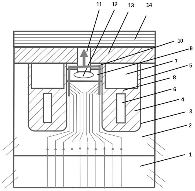
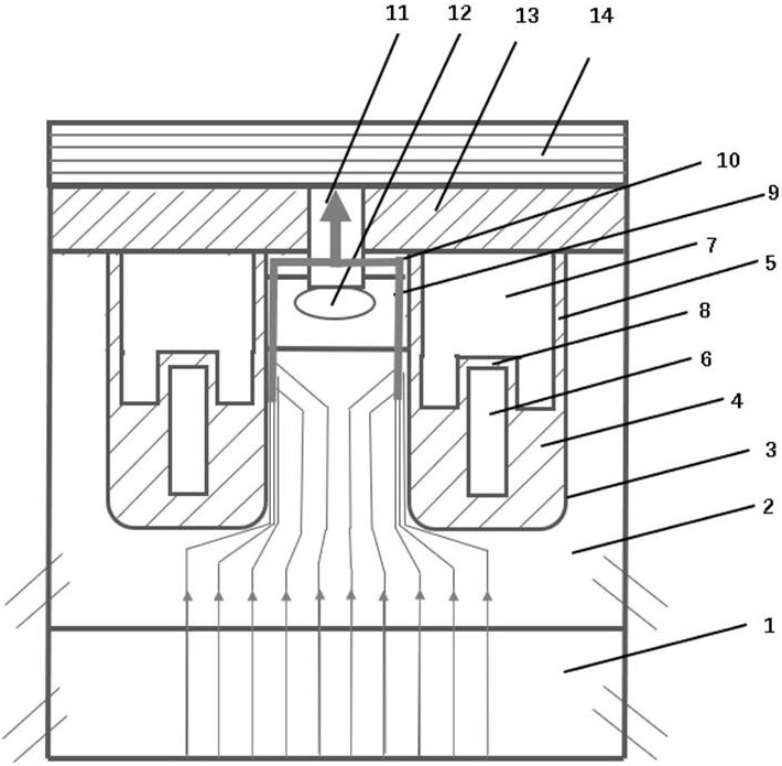
[0023] The invention relates to a low on-resistance deep trench MOSFET device structure, the device comprises a first conductivity type high concentration doped silicon substrate 1 contacting the back drain and a first conductivity type high concentration doped silicon substrate 1 A low-concentration doped silicon epitaxial layer 2 of the first conductivity type on the substrate 1, a deep trench 3 is arranged in the low-concentration doped silicon epitaxial layer 2 of the first conductivity type, and the deep trench 3 is wrapped The field oxide layer 4 on the lower layer and the gate oxide layer 5 on the upper layer are respectively provided with the shield gate polysilicon 6 on the lower layer and the gate polysilicon on the upper layer between the field oxide layers 4 and the gate oxide layers 5 7. An oxide layer 8 is provided between the shielded gate polysilicon 6 and...


PUM


Abstract

The invention relates to a deep trench MOSFET device structure with low on-resistance. The deep trench MOSFET device structure is characterized in that the shielded gate electrode polysilicon of the device is in short circuit with gate electrode polysilicon above the shielded gate electrode polysilicon, an accumulation layer is formed in an MESA region close to a deep trench region, and the left side and the right side of the gate electrode polysilicon extend downwards to form a low-resistance region on the side wall of the deep trench. According to the invention, the traditional short circuitbetween the shielded gate electrode and the source region is improved into the short circuit between the shielded gate electrode and the gate electrode, so that the dielectric between the polysilicons is reduced to the minimum, the upper gate electrode polycrystalline silicon layer extends downwards, and part of MESA resistance of the device is converted into accumulation layer resistance with lower resistivity; and through the extension of the gate electrode polycrystalline silicon layer, the equipotential line in the MESA is transferred to the middle position of the deep trench from the PNjunction between the body region and the drift region, so that the longitudinal electric field intensity of the deep trench MOSFET platform is converted into more uniform approximate rectangular distribution from hump distribution.

Description

technical field [0001] The invention relates to the technical field of semiconductor power devices, in particular to a low on-resistance deep trench MOSFET device structure. Background technique [0002] In the field of medium and low voltage power devices with a withstand voltage lower than 250V, deep trench MOSFET devices are widely used due to their low characteristic on-resistance and moderate process complexity. The deep trench MOSFET device uses the shielded gate as the internal field plate to reduce the electric field in the drift region, so as to achieve the purpose of reducing the resistance of the drift region and the characteristic on-resistance. [0003] Due to the fact that the shielded gate occupies a large amount of space in the drift region and the resistivity of the drift region is still relatively high, among the many components of the on-resistance of deep trench MOSFET devices, the MESA resistance accounts for a large proportion, which hinders the charact...

Claims


Application Information

Patent Timeline
Patent Type & Authority Applications(China)
IPC IPC(8): H01L29/423H01L29/78
CPCH01L29/4236H01L29/7827H01L29/7831
Inventor 李恩求李铁生杨乐刘琦
Owner XIAN LONTEN RENEWABLE ENERGY TECH
Why Eureka
Try Eureka