Device and method for removing nanoscale particles adsorbed on surface of silicon wafer

A silicon wafer surface, nano-scale technology, applied in the direction of using liquid cleaning methods, cleaning methods and utensils, chemical instruments and methods, etc., can solve the problems of device structure damage, difficult particle removal, secondary pollution, etc. Small size, low cost, convenient installation and debugging

Active Publication Date: 2021-01-29
HUAZHONG UNIV OF SCI & TECH
View PDF6 Cites 0 Cited by
  • Summary
  • Abstract
  • Description
  • Claims
  • Application Information

AI Technical Summary

Problems solved by technology

At present, the main technology of pollution particle removal research is fluid removal technology. Its principle is to use fluid to impact pollution particles to generate removal force, and then realize the removal of pollution particles, such as high-pressure liquid jet flow, high-pressure gas jet flow, etc., but the fluid acc...

Method used


Image

  • Device and method for removing nanoscale particles adsorbed on surface of silicon wafer
  • Device and method for removing nanoscale particles adsorbed on surface of silicon wafer

Examples


Embodiment Construction

[0026] In order to make the object, technical solution and advantages of the present invention clearer, the present invention will be further described in detail below in conjunction with the accompanying drawings and embodiments. It should be understood that the specific embodiments described here are only used to explain the present invention, not to limit the present invention. In addition, the technical features involved in the various embodiments of the present invention described below can be combined with each other as long as they do not constitute a conflict with each other.

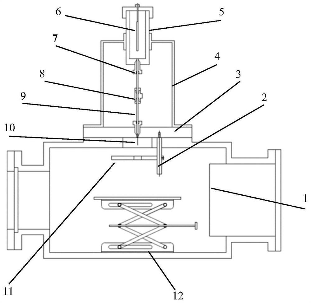
[0027] see figure 1 and figure 2 The present invention provides a device for removing adsorbed nanoscale particles on the surface of a silicon wafer, which includes a vacuum component, a vertical lifting platform 12 arranged in the vacuum component, and a droplet launching and accelerating component connected to the vacuum component. The vacuum assembly includes a vacuum chamber 1 , a hot cat...


PUM


Abstract

The invention belongs to the related technical field of semiconductor surface cleaning, and discloses a device and method for removing nanoscale particles adsorbed on the surface of a silicon wafer. The device comprises a vacuum assembly and a liquid drop emission and acceleration assembly connected to the vacuum assembly; the liquid drop emission and acceleration assembly comprises a liquid storage device, a graphite electrode, a PEEK capillary tube, a fused quartz capillary tube and a grounded extraction electrode; the liquid storage device is arranged above the vacuum assembly and is used for accommodating a conductive solution; the graphite electrode is arranged on the liquid storage device, and two ends of the graphite electrode are connected with a direct-current power supply and theconductive liquid; one end of the PEEK capillary tube is connected with the liquid storage device, the other end of the PEEK capillary tube is connected with the fused quartz capillary tube, and oneend of the fused quartz capillary tube extends into the vacuum assembly; and the extraction electrode is arranged in the vacuum assembly and is opposite to the emission tip formed by the fused quartzcapillary tube. According to the device and method, the cleaning efficiency is improved, the cost is reduced, and no liquid is left after removal.

Description

technical field [0001] The invention belongs to the technical field related to semiconductor surface cleaning, and more specifically relates to a device and method for removing adsorbed nanoscale particles on the surface of a silicon wafer. Background technique [0002] The integrated circuit industry reflects the level of a country's high-end manufacturing industry. The current emerging industries such as cloud computing, Internet of Things, and big data have greatly promoted the demand for integrated circuit chips. For example, China imports about 200 billion US dollars of chips every year, which has exceeded its oil imports. It is the largest chip consumption market in the world, and only 16% of them are localized. The integrated circuit industry is related to national security and is still a weak link in the manufacturing industry. The bottleneck technology surrounding the integrated circuit industry has become a problem that scientific researchers urgently need to overc...

Claims


Application Information

Patent Timeline
IPC IPC(8): B08B3/02B08B13/00H01L21/02
CPCB08B3/02B08B13/00H01L21/02041
Inventor 许剑锋张吉韬贾凯
Owner HUAZHONG UNIV OF SCI & TECH
Why Eureka
Try Eureka