Schottky diode with deep energy level doping

A Schottky diode, deep-level impurity technology, applied in electrical components, circuits, semiconductor devices, etc., can solve problems such as low leakage current, achieve low leakage current, reduce high temperature leakage current, and reduce device power consumption.

Pending Publication Date: 2021-01-29
广微集成技术(深圳)有限公司
View PDF0 Cites 0 Cited by
  • Summary
  • Abstract
  • Description
  • Claims
  • Application Information

AI Technical Summary

Problems solved by technology

[0006] The technical problem to be solved by the present invention is to provide a Schottky diode with deep level doping that can obtain lower leakage current and does not affect the forward voltage drop of the device at normal temperature

Method used


Image

  • Schottky diode with deep energy level doping

Examples


Embodiment Construction

[0015] In order to make those skilled in the art more clearly understand the purpose, technical solutions and advantages of the present invention, the present invention will be further described below in conjunction with the accompanying drawings and embodiments.

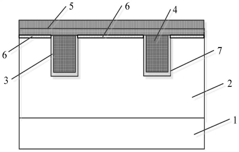
[0016] refer to figure 1 , figure 1 It is a structural schematic diagram of a specific embodiment of the Schottky diode with deep level doping in the present invention. In the embodiment shown in the accompanying drawings, the Schottky diode includes a substrate 1 and an epitaxial layer 2 formed on the surface of the substrate 1. The epitaxial layer 2 is provided with several grooves 7, and each groove A gate oxide layer 3 is formed on the inner wall and bottom of the trench 7, and the trench 7 is filled with polysilicon 4, and the polysilicon 4 covers the gate oxide layer 3 in a plurality of trenches 7, and each trench 7 is surrounded by a The deep level impurity layer 6 , the metal layer 5 is formed on the upper...


PUM


Abstract

The invention discloses a Schottky diode with deep energy level doping, which comprises a substrate and an epitaxial layer formed on the surface of the substrate, wherein a plurality of grooves are formed on the epitaxial layer, gate oxide layers are formed on the inner side wall and the bottom part of each groove, polycrystalline silicon is filled in the grooves, the polycrystalline silicon covers the gate oxide layers in the plurality of grooves, a deep energy level impurity layer is formed beside each groove, and metal layers are formed on the deep energy level impurity layers and the uppersurfaces of the grooves. According to the Schottky diode, the deep energy level impurity layer is formed beside each groove, the metal layers are formed on the deep energy level impurity layers and the upper surfaces of the grooves, impurities in the deep energy level impurity layers cannot be completely activated under the condition of normal temperature, the barrier of the diode is low, and theforward voltage drop is low; and under the condition of high temperature, most of impurities are activated, so that the barrier height of the Schottky diode can be effectively improved, the high-temperature leakage current of the Schottky diode is reduced, and the power consumption of the device is further reduced.

Description

technical field [0001] The invention relates to the technical field of semiconductor devices, in particular to a Schottky diode with deep level doping. Background technique [0002] As we all know, the Schottky diode named after the inventor Dr. Schottky (Schottky) is made by using the metal-semiconductor barrier principle formed by the contact between metal and semiconductor. It is a low-power, high-current, ultra-high-speed semiconductor device. , Its notable feature is that the reverse recovery time is extremely short (it can be as small as a few nanoseconds), the forward voltage drop is only about 0.4V, and the rectification current can reach several thousand amperes. [0003] Due to the barrier lowering effect of the Schottky diode itself, the Schottky diode will generate a large leakage current at high voltage, which is the main reason for limiting the application of the Schottky diode in the high voltage field. In recent years, with the successful marketization of TM...

Claims


Application Information

Patent Timeline
IPC IPC(8): H01L29/872H01L29/06H01L21/329
CPCH01L29/0619H01L29/66143H01L29/8725
Inventor 单亚东谢刚
Owner 广微集成技术(深圳)有限公司
Why Eureka
Try Eureka