
Eureka
For R&D, Eureka makes reading and utilizing patents & technical documents easy.
Eureka AIR
Designed for self-driven R&D workflows. Generate viable solutions, solve complex R&D challenges, empower your innovation with AI.

Eureka Materials
Designed for material experts only. Revolutionize your material R&D, from search, analyze, to developing new materials.

TechResearch
Generate reliable direction feasibility study reports for your R&D in just a few steps.

TechSeek
Discover and master advanced knowledge NOW. Basics, ideas, possibilities, all at once.

TechMind
As an expert in R&D Theories, TechMind can generates customized viable solutions instantly.

TechRisk
Analyze your overall solution with one click, know your potential R&D risks in advance.

TechMonitor
Get weekly tech updates, stay abreast of the latest tech innovations and key insights.
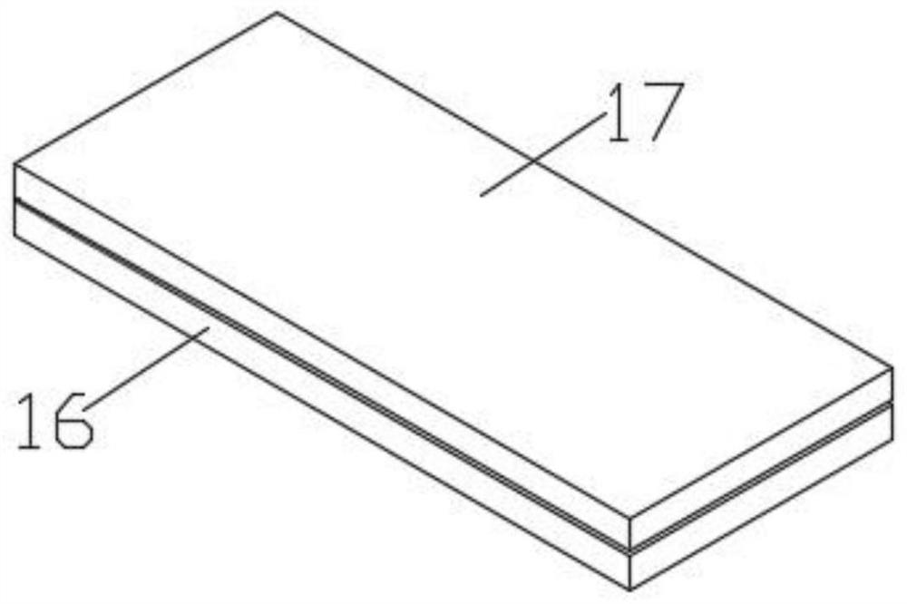
Ceramic substrate for integrated packaging
A ceramic substrate, integrated packaging technology, applied in electrical components, circuits, electrical solid devices and other directions, can solve the problems of low thermal conductivity, low cutting efficiency, affecting the service life of components, etc., to achieve the effect of optimizing physical and chemical properties
- Summary
- Abstract
- Description
- Claims
- Application Information
AI Technical Summary
Problems solved by technology
Method used
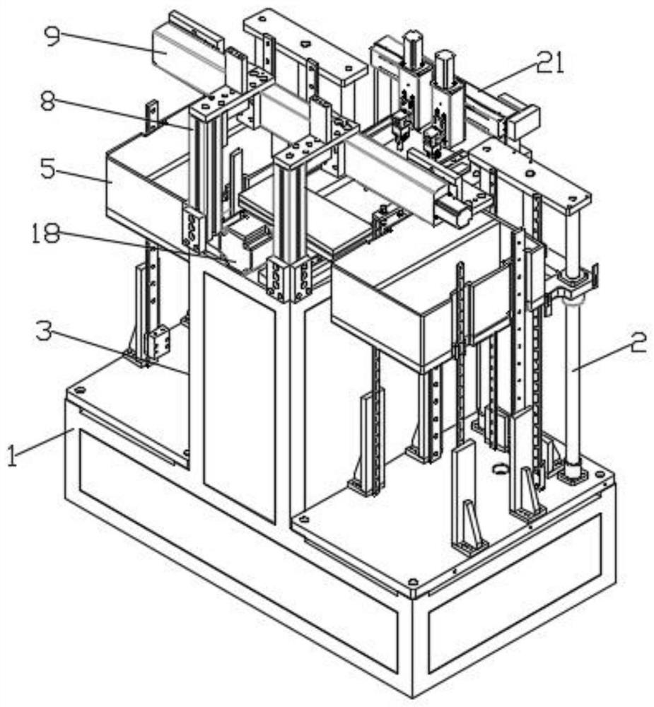
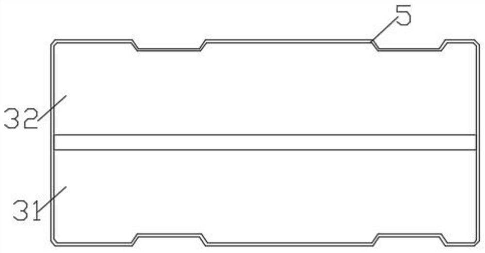
Image

Examples
Embodiment 1
[0042] A ceramic substrate for integrated packaging, prepared from the following raw materials in parts by weight: 30 parts of aluminum nitride, 30 parts of boron nitride, 30 parts of aluminum oxide, 10 parts of beryllium oxide, 5 parts of glass sintering aids, copper aluminum 5 parts of alloy nanoparticles, 2 parts of rare earth oxide, 5 parts of organic solvent, 1 part of plasticizer, 1 part of dispersant, and 1 part of binder;
[0043] Wherein, the ceramic substrate for integrated packaging is prepared through the following steps:
[0044] Step 1: Add aluminum nitride, boron nitride, aluminum oxide, beryllium oxide, copper aluminum alloy nanoparticles, rare earth oxides, organic solvents, plasticizers, dispersants, binders, and glass sintering aids into the ball mill, Wet ball milling for 3 hours to prepare ceramic slurry;
[0045] Step 2: Press the ceramic slurry into the mold, gel and dry to obtain the ceramic green sheet;
[0046] Step 3: Put the ceramic green sheet in...
Embodiment 2
[0051] A ceramic substrate for integrated packaging, prepared from the following raw materials in parts by weight: 40 parts of aluminum nitride, 40 parts of boron nitride, 40 parts of aluminum oxide, 20 parts of beryllium oxide, 10 parts of glass sintering aids, copper aluminum 10 parts of alloy nanoparticles, 5 parts of rare earth oxides, 10 parts of organic solvents, 2 parts of plasticizers, 2 parts of dispersants, and 2 parts of binders;
[0052]Wherein, the ceramic substrate for integrated packaging is prepared through the following steps:
[0053] Step 1: Add aluminum nitride, boron nitride, aluminum oxide, beryllium oxide, copper aluminum alloy nanoparticles, rare earth oxides, organic solvents, plasticizers, dispersants, binders, and glass sintering aids into the ball mill, Wet ball milling for 5 hours to prepare ceramic slurry;
[0054] Steps 2, 3 and 4 are the same as in Example 1.
[0055] Specifically, the glass sintering aid is prepared by the following steps: We...
PUM
| Property | Measurement | Unit |
|---|---|---|
| particle diameter | aaaaa | aaaaa |
| particle diameter | aaaaa | aaaaa |
Abstract
Description
Claims
Application Information
 - R&D Engineer
- R&D Manager
- IP Professional
- Industry Leading Data Capabilities
- Powerful AI technology
- Patent DNA Extraction
Browse by: Latest US Patents, China's latest patents, Technical Efficacy Thesaurus, Application Domain, Technology Topic, Popular Technical Reports.
© 2024 PatSnap. All rights reserved.Legal|Privacy policy|Modern Slavery Act Transparency Statement|Sitemap|About US| Contact US: help@patsnap.com