High-precision etching production system and method for flexible PCB

A PCB board and production method technology, applied to flexible printed circuit boards, removal of conductive materials by chemical/electrolytic methods, sequence of processing steps, etc., can solve the difficulty of debugging process parameters, large amount of side erosion of fine lines, and circuit Problems such as poor microscopic morphology, to achieve the effect of simplifying process parameter debugging, improving production efficiency and yield, and difficult

Inactive Publication Date: 2021-02-23
WUHAN UNIV
View PDF5 Cites 8 Cited by
  • Summary
  • Abstract
  • Description
  • Claims
  • Application Information

AI Technical Summary

Problems solved by technology

[0005] The present invention aims at problems such as large amount of side erosion of fine lines, low etching factor, poor microscopic appearance of lines, and low yield of finished products, which are difficult to debug process parameters in the existing fine circuit PCB production process, and proposes a method for reducing It is difficult to debug process parameters, and the etching process method to improve the quality and yield of fine PCB lines

Method used


Image

  • High-precision etching production system and method for flexible PCB
  • High-precision etching production system and method for flexible PCB
  • High-precision etching production system and method for flexible PCB

Examples


Embodiment Construction

[0043] In order to fully illustrate the technical content of the present invention, the technical solutions of the present invention will be further introduced and described below in conjunction with specific implementation methods and accompanying drawings.

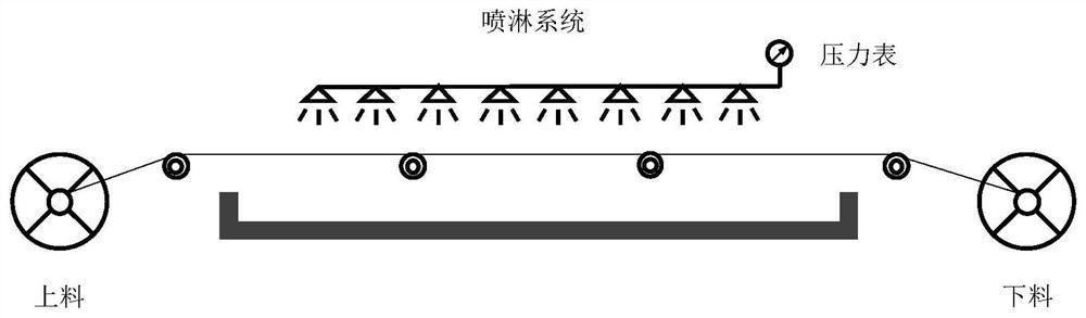
[0044] figure 1 It is a schematic diagram of the production line structure of the traditional etching process for fine PCB boards, refer to figure 1 , the traditional etching process uses the same process production parameters for the entire spray equipment, that is, the spray pressure, spray temperature, solution concentration and other parameters are the same for the entire production line, which can easily cause uneven etching of the line, serious side erosion, etc. The problem greatly affects the accuracy and quality of the fine PCB board.

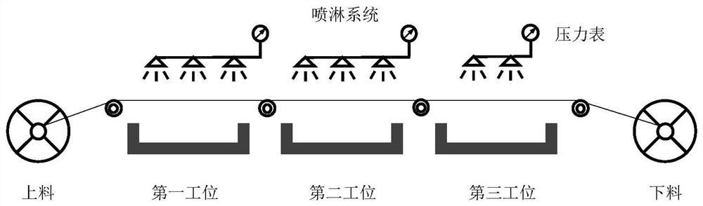
[0045] figure 2 It is a structural schematic diagram of a high-precision etching production system for flexible PCB boards proposed by the present invention, including a PCB...


PUM

PropertyMeasurementUnit
thicknessaaaaaaaaaa
thicknessaaaaaaaaaa
thicknessaaaaaaaaaa

Abstract

The invention discloses a high-precision etching production system and method for a flexible PCB. The system comprises a PCB substrate feeding device, a line body conveying device and a finished product discharging device, the line body conveying device is provided with a plurality of etching stations in the line body conveying direction, and a spraying system for independently controlling parameters is disposed above each etching station. The PCB substrate feeding device is used for feeding exposed and developed PCB substrates to the line body conveying device, the PCB substrates pass throughthe three etching stations in sequence through line body conveying, the spraying pressure of the three etching stations is gradually increased, the concentration of etching liquid is gradually reduced, a large amount of etching of metal etching layers on the PCB substrates is completed through different parameters, and basic forming etching and high-precision forming etching are carried out, so that high-precision etching production of the flexible PCB is completed. The system and the method are simple in structure, high in production efficiency, high in etching precision and suitable for mass production of high-precision miniature circuit boards, and the efficiency of an existing production line can be greatly improved by modifying the prior art.

Description

technical field [0001] The invention belongs to the field of optoelectronics, and relates to a PCB manufacturing technology, in particular to a high-precision etching production system and method of a flexible PCB board. Background technique [0002] Flexible PCB is a printed circuit board made of flexible substrates, which has the characteristics of high reliability and excellent flexibility. The production process of flexible PCB is generally: I-type punching→coating→exposure→developing→etching→removing film→tinning→automatic optical inspection→ink printing→slitting→circuit inspection→final cleaning and packaging. Among them, the etching process plays a decisive role in the final quality of PCB products. [0003] At present, flexible PCB has been widely used in terminal consumption fields such as smartphones, automobiles, and wearable devices. With the rapid development of high integration and high precision of internal components such as personal computers and smartphone...

Claims


Application Information

Patent Timeline
Patent Type & Authority Applications(China)
IPC IPC(8): H05K3/06
CPCH05K3/061H05K2201/05H05K2203/0736H05K2203/14
Inventor 李辉盛家正申胜男
Owner WUHAN UNIV
Why Eureka
Try Eureka