A high-efficiency perovskite photonic crystal laser
A photonic crystal, photonic crystal microcavity technology, applied in the field of nano-laser
- Summary
- Abstract
- Description
- Claims
- Application Information
AI Technical Summary
Problems solved by technology
Method used
Image
Examples
Embodiment example
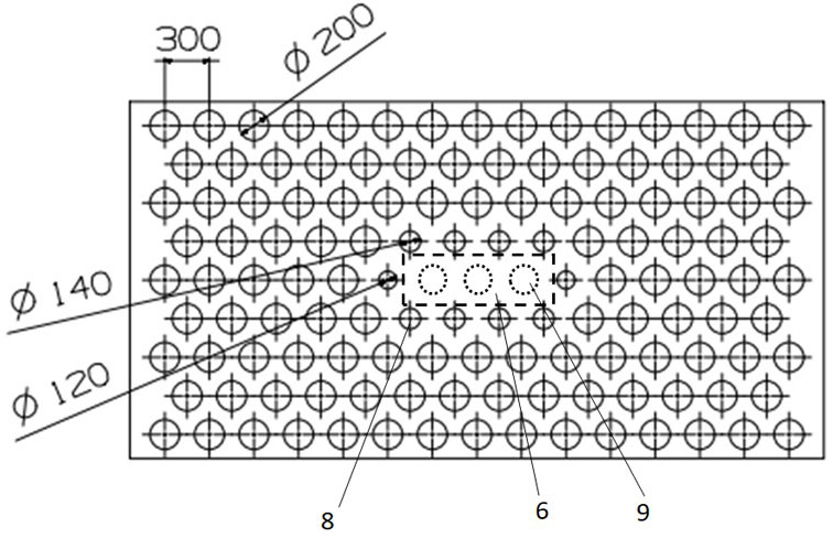
[0020] Implementation case: This example uses CH 3 NH 3 PB 3 Nanosheets are taken as an example for further explanation. TiO 2 The specific process of preparing the photonic crystal resonator is as follows: first, the photonic crystal nano-resonator mold is prepared on the silicon substrate by electron beam etching. The microstructural parameters of the mold are as follows: the lattice constant a is 300 nm, and the air hole radius is 100 nm, the air holes near both ends of the defect move 36 nm outward to both ends, the pore diameter is reduced to 60 nm, the radius of the air holes on the upper and lower sides of the defect is 70 nm, and the depth is 200 nm. Then the PDMS anti-template was prepared by pouring and demoulding. Then the TiO needed for the experiment was prepared by nanoimprinting technique. 2 Photonic crystal air thin film, the specific process is: Spin coating TiO on the PDMS counter template 2 The precursor solution, after the solvent is evaporated by hea...
PUM
| Property | Measurement | Unit |
|---|---|---|
| radius | aaaaa | aaaaa |
| radius | aaaaa | aaaaa |
| thickness | aaaaa | aaaaa |
Abstract
Description
Claims
Application Information


