Absorption film based on atomic layer deposition and manufacturing method thereof
An atomic layer deposition and absorption film technology, applied in the field of absorption film, can solve the problems of difficult to achieve full coverage, limited film uniformity, etc., and achieve the effects of good incident angle insensitivity, convenient preparation method, and good uniformity.
- Summary
- Abstract
- Description
- Claims
- Application Information
AI Technical Summary
Problems solved by technology
Method used
Image
Examples
preparation example Construction
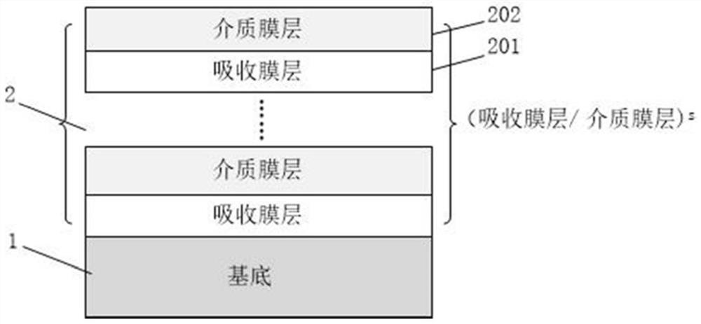
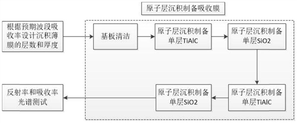
[0042] The preparation of the absorption film based on atomic layer deposition is mainly realized by adjusting the layer number and thickness of the atomic layer deposition absorption layer and dielectric layer material. Such as figure 2 As shown, the preparation process of the absorbing film based on atomic layer deposition is as follows:
[0043] (1) According to the absorption film material, dielectric film material and substrate material, as well as the requirements for the bandwidth and absorption rate of the absorber, using optical design software, by optimizing the thickness of each layer of film, design a visible-near optical film that can achieve the corresponding absorption characteristics. Infrared band absorbing film system.
[0044] (2) To clean the substrate, the substrate can be wiped with an ethanol / ether mixed solution, or the substrate can be cleaned by solution ultrasonic method: first, the substrate is ultrasonically cleaned in acetone solution, and then ...
Embodiment 1
[0058] Example 1: The specific film structure in the visible light band is preferably substrate|TiAlC(15nm)|SiO 2 (41nm)|TiAlC(240nm)|SiO 2 (17nm)|TiAlC(23nm)|SiO 2 (63nm), such as Figure 5 shown. The final equivalent admittance of the film system matches the admittance of the incident medium air, and when the incident beam is reflected on the surface of the film layer, it will produce a destructive interference effect, thereby reducing the reflection loss on the film system surface. When incident from the air side, the average reflectance of the visible light band 400-700nm is as low as 0.39%, such as Image 6 As shown in (a); when incident from the base side, the average reflectance of the visible light band 400-700nm is 0.91%, as Image 6 Shown in (b).
[0059] Absorption film structure substrate|TiAlC(15nm)|SiO 2 (41nm)|TiAlC(240nm)|SiO 2 (17nm)|TiAlC(23nm)|SiO 2 (63nm), the titanium-aluminum chemical compound TiAlC near the substrate is used as the absorbing laye...
Embodiment 2
[0060] Example 2: The absorbing film in the visible-near-infrared band is designed with total absorption in the 400-1100nm band, and the specific absorbing film structure is preferably substrate|TiAlC(10nm)|SiO 2 (60nm)|TiAlC(30nm)|SiO 2 (42nm)|TiAlC(230nm)|SiO 2 (28nm)|TiAlC(34nm)|SiO 2 (43nm)|TiAlC(21nm)|SiO 2 (80nm), such as Figure 8 As shown, when incident from the air side, the average reflectance of visible light-near infrared band 400-1100nm is as low as 0.77%, as Figure 9 As shown in (a); when incident from the base side, the average reflectance of visible light-near infrared band 400-1100nm is 0.50%, as Figure 9 Shown in (b).
[0061] Its absorption in the visible-near-infrared band is significantly increased. Since the middle absorbing layer is thick enough, no light is transmitted through the device, and the anti-reflection combination of the upper and lower layers further reduces the reflection loss in this band and improves the absorption efficiency. - Hi...
PUM
| Property | Measurement | Unit |
|---|---|---|
| thickness | aaaaa | aaaaa |
| thickness | aaaaa | aaaaa |
| thickness | aaaaa | aaaaa |
Abstract
Description
Claims
Application Information


