A kind of distributed feedback laser and its preparation method

A distributed feedback, laser technology, applied in the field of lasers, can solve the problem of the difference of the conduction band energy level affecting the performance of the device, and achieve the effect of improving the performance of the device, reducing the resistance, and reducing the size of the parasitic resistance.

Active Publication Date: 2022-04-19
SUZHOU EVERBRIGHT PHOTONICS CO LTD +1
View PDF13 Cites 0 Cited by
  • Summary
  • Abstract
  • Description
  • Claims
  • Application Information

AI Technical Summary

Problems solved by technology

[0004] Therefore, the technical problem to be solved by the present invention is to overcome the defect in the prior art that the large difference in the conduction band energy level of InP and InGaAlAs affects the performance of the device, thereby providing a distributed feedback laser and its preparation method

Method used


Image

  • A kind of distributed feedback laser and its preparation method
  • A kind of distributed feedback laser and its preparation method
  • A kind of distributed feedback laser and its preparation method

Examples


Embodiment 1

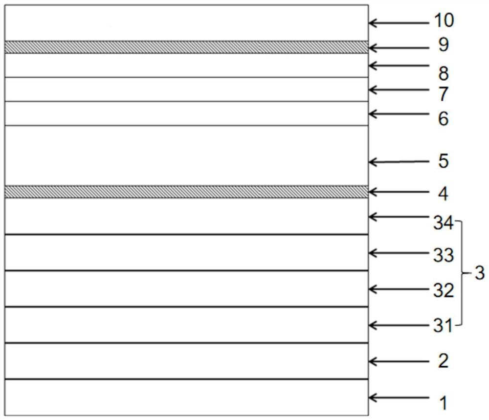
[0063] This embodiment provides a distributed feedback laser, refer to figure 2 , including a stacked second electrode (not shown in the figure), an InP substrate 1, an N-type InP buffer layer 2, an InGaAlAs semiconductor layer 3, a first P-type insertion layer 4, a P-type InP transition layer 5, and a grating layer 6. The grating cover layer 7, the P-type InP optical confinement layer 8, the P-type InGaAs ohmic contact layer 10 and the first electrode (not shown in the figure), wherein the first P-type insertion layer 4 is (InGaAlAs) 1-x (InP) x Material. The InGaAlAs semiconductor layer 3 includes a stacked N-type InGaAlAs confinement layer 31, an undoped InGaAlAs first waveguide layer 32, an undoped InGaAlAs active layer 33, and an undoped InGaAlAs second waveguide layer 34. The undoped InGaAlAs The doped InGaAlAs second waveguide layer 34 is disposed between the non-doped InGaAlAs active layer 33 and the first P-type insertion layer 4 .

[0064] In the above-mentioned ...

Embodiment 2

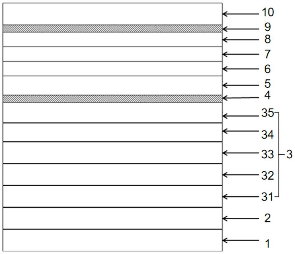
[0118] This embodiment provides a distributed feedback laser, refer to image 3 , including a stacked second electrode (not shown in the figure), an InP substrate 1, an N-type InP buffer layer 2, an InGaAlAs semiconductor layer 3, a first P-type insertion layer 4, a P-type InP transition layer 5, and a grating layer 6. A grating covering layer 7, a P-type InP optical confinement layer 8, a P-type InGaAs ohmic contact layer 10, and a first electrode (not shown in the figure), wherein the first P-type insertion layer 4 is (InGaAlAs) 1-x (InP) xMaterial. The InGaAlAs semiconductor layer 3 includes an N-type InGaAlAs confinement layer 31, a non-doped InGaAlAs first waveguide layer 32, a non-doped InGaAlAs active layer 33, a non-doped InGaAlAs second waveguide layer 34 and a P-type InGaAlAs confinement layer 31. layer 35, the P-type InGaAlAs confinement layer 35 is disposed between the non-doped InGaAlAs second waveguide layer 34 and the first P-type insertion layer 4, and the P-...


PUM

PropertyMeasurementUnit
thicknessaaaaaaaaaa

Abstract

The invention provides a distributed feedback laser and a preparation method thereof. The distributed feedback laser comprises: an InGaAlAs semiconductor layer; a P-type InP transition layer; a first P-type insertion layer located between the InGaAlAs semiconductor layer and the P-type InP transition layer, The first P-type insertion layer is (InGaAlAs) 1-x (InP) x Material. By disposing the first P-type insertion layer between the InGaAlAs semiconductor layer and the P-type InP transition layer, the absolute value of the conduction band energy step difference between the InGaAlAs semiconductor layer and the P-type InP transition layer is converted into the first P-type insertion layer and the sum of the absolute value of the conduction band energy level difference of the InGaAlAs semiconductor layer and the absolute value of the conduction band energy level difference between the first P-type insertion layer and the P-type InP transition layer, thereby reducing the size of the introduced parasitic resistance and improving the Device performance of distributed feedback lasers.

Description

technical field [0001] The invention relates to the technical field of lasers, in particular to a distributed feedback laser and a preparation method thereof. Background technique [0002] As the commercialization of 5G is approaching, the dynamic single-mode distributed feedback laser (DFB-LD) with narrow linewidth, high side mode suppression ratio and high modulation rate has become the preferred light source. Distributed feedback laser adopts grating modulation with periodically changing refractive index, has good single longitudinal mode characteristic, side mode suppression ratio can reach more than 50dB, and modulation rate can reach more than 50Gb / s, which can meet the high speed / low time requirement of 5G mobile network. Delayed application requirements. Distributed feedback lasers for high-speed optical communication generally use InP as the growth substrate, and use InGaAlAs quantum wells as the active layer. [0003] However, due to the large difference between ...

Claims


Application Information

Patent Timeline
Patent Type & Authority Patents(China)
IPC IPC(8): H01S5/12H01S5/32H01S5/323
CPCH01S5/12H01S5/321H01S5/32391H01S2304/04
Inventor 郭银涛王俊程洋肖啸
Owner SUZHOU EVERBRIGHT PHOTONICS CO LTD
Why Eureka
Try Eureka