Semiconductor device for preventing surface metal layer from desoldering and manufacturing method thereof

A technology of surface metal layer and manufacturing method, which is applied in semiconductor/solid-state device manufacturing, semiconductor devices, semiconductor/solid-state device components, etc., can solve problems such as falling off, peeling, damage, and insufficient welding reliability, and achieve high reliability , It is not easy to fall off, and the effect of improving reliability

Inactive Publication Date: 2021-03-23
上海擎茂微电子科技有限公司
View PDF4 Cites 0 Cited by
  • Summary
  • Abstract
  • Description
  • Claims
  • Application Information

AI Technical Summary

Problems solved by technology

[0003] However, in semiconductor power devices, there is often insufficient welding reliability between the aluminum wire and the metal layer on the surface of the chip during chip bonding, and the surface metal layer (aluminum, copper, aluminum-silicon-copper alloy or aluminum-copper alloy, etc.) Shedding, peeling, and even the destruction of the ILD (insulating interlayer dielectric) layer on the surface of the chip, which seriously affects the reliability of the power device chip

Method used


Image

  • Semiconductor device for preventing surface metal layer from desoldering and manufacturing method thereof

Examples


Embodiment Construction

[0027] The specific implementation manners of the present invention will be further described in detail below in conjunction with the accompanying drawings and embodiments. The following examples are used to illustrate the present invention, but are not intended to limit the scope of the present invention.

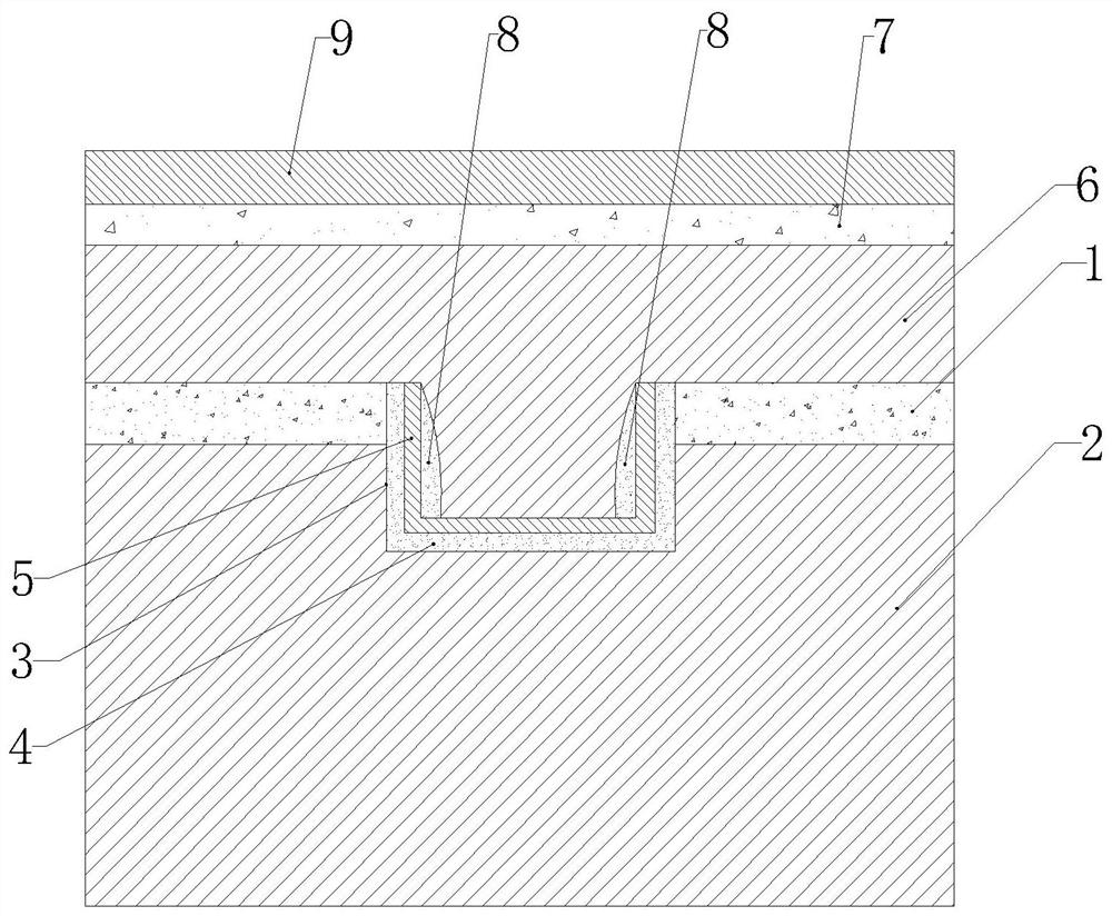
[0028] see figure 1 A semiconductor device for preventing desoldering of the surface metal layer according to a preferred embodiment of the present invention includes a semiconductor device 2 with an insulating dielectric layer 1 on the surface, a contact hole 3 is provided on the surface of the semiconductor device, and a layer composed of The contact layer 4 is made of metal titanium, the surface of the contact layer is provided with a layer of barrier layer 5 made of titanium nitride material, and the inner surface of the contact hole is also provided with a layer of side wall protection layer 8 made of metal tungsten material, A metal interconnection layer 6 is also p...


PUM


Abstract

The invention relates to a semiconductor device for preventing a surface metal layer from desoldering, which comprises a semiconductor device with an insulating dielectric layer on the surface, wherein a contact hole is arranged on the surface of the semiconductor device, a contact layer made of a metal titanium material is arranged on the inner side surface of the contact hole, a barrier layer made of a titanium nitride material is arranged on the surface of the contact layer, a side wall protection layer made of a metal tungsten material is further arranged on the inner side surface of the contact hole, a metal interconnection layer is further arranged in the contact hole and on the surface of the semiconductor device, and a first passivation layer and a second passivation layer are arranged above the metal interconnection layer. According to the semiconductor device for preventing the surface metal layer from desoldering, the surface metal layer is not easy to fall off and peel offafter bonding, and the reliability is high. In addition, the invention also relates to a manufacturing method of the semiconductor device.

Description

technical field [0001] The present invention relates to a semiconductor device, in particular to a semiconductor device that prevents desoldering of a surface metal layer, and also relates to a manufacturing method of the semiconductor device. Background technique [0002] In the semiconductor manufacturing process, the metal process and passivation process on the surface of the semiconductor structure are key technologies. Among them, in the packaging process, the metal layer on the surface of the general device will bear a lot of stress when the wire is bonded. In order to prevent the stress of the metal wires from affecting the performance of the semiconductor device, multiple metal layers or thicker metal layers are generally used to buffer the stress. In addition, by forming a passivation layer on the surface of the semiconductor structure, various charges in the oxide layer inside the semiconductor structure can be reduced, the ability of the semiconductor structure t...

Claims


Application Information

Patent Timeline
Patent Type & Authority Applications(China)
IPC IPC(8): H01L23/482H01L23/485H01L21/48
CPCH01L23/4827H01L23/485H01L21/4814
Inventor 王海军阳平
Owner 上海擎茂微电子科技有限公司
Why Eureka
Try Eureka