

Mask blank and photomask
A technology of mask blanks and photomasks, applied in optics, originals for photomechanical processing, ion implantation plating, etc., can solve the problem of poor etching rate between the light-shielding layer and the anti-reflection layer, non-progressive etching of the anti-reflection layer, Problems such as low etch rate of anti-reflection layer etch rate
- Summary
- Abstract
- Description
- Claims
- Application Information
AI Technical Summary
Problems solved by technology
Method used
Image

Examples
Embodiment 1
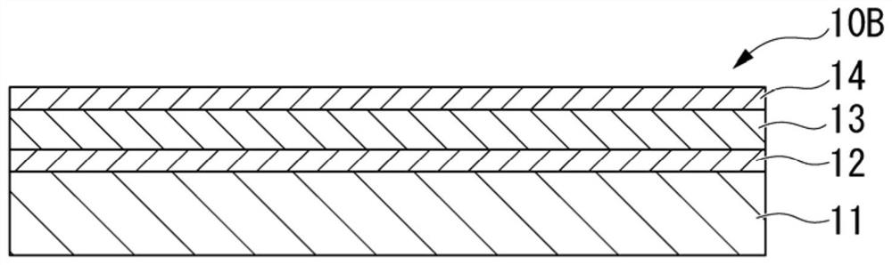
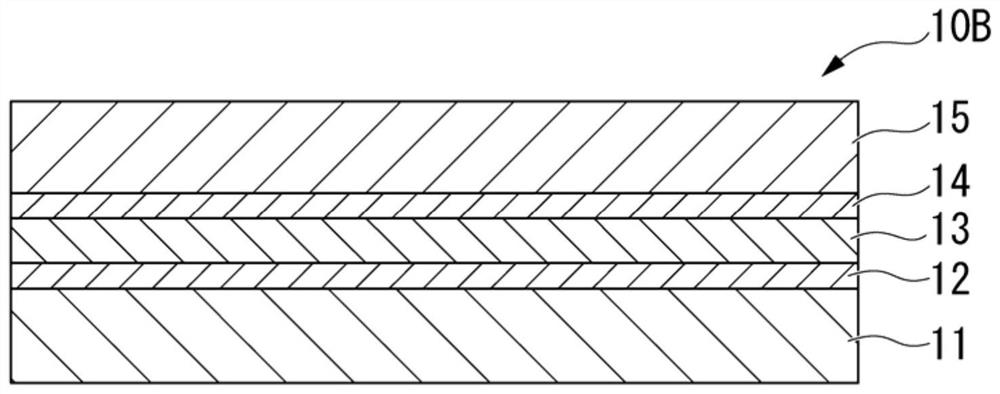
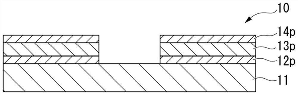
[0169] A film of a chromium compound as a three-layer mask layer was formed on a glass substrate using a sputtering method.
[0170] When forming the chromium compound film as the light-shielding layer, sputtering is performed with nitrogen gas.
[0171] Nitrogen gas was used to sputter when forming the chromium compound film as the upper and lower antireflection layers. In addition, as the oxidizing gas, choose CO 2 gas and NO gas, and change the partial pressure of each gas. Show its gas ratio in figure 1 .
[0172] [Table 1]
[0173]
[0174] In addition, Table 2 shows the film thickness of the lower antireflection layer 12 , the film thickness of the light shielding layer 13 , the film thickness of the upper antireflection layer 14 , and the total film thickness of the mask layer.
[0175] [Table 2]
[0176]
[0177] Changes in the composition ratios of N, O, Cr, and C in each layer of Example 1 were determined by Auger electron spectroscopy. The results are s...
Embodiment 2
[0188] A film of a chromium compound as a three-layer mask layer was formed on a glass substrate using a sputtering method.
[0189] When forming the chromium compound film as the light-shielding layer, sputtering is performed with nitrogen gas.
[0190] Nitrogen gas was used to sputter when forming the chromium compound film as the upper and lower antireflection layers. In addition, as the oxidizing gas, choose CO 2 gas and NO gas, and change the partial pressure of each gas. The gas ratio is shown in Table 1.
[0191] In addition, Table 2 shows the film thickness of the lower antireflection layer 12 , the film thickness of the light shielding layer 13 , the film thickness of the upper antireflection layer 14 , and the total film thickness of the mask layer.
[0192] Changes in the composition ratios of N, O, Cr, and C in each layer of Example 2 were determined by Auger electron spectroscopy. The results are shown in Table 6.
[0193] [Table 6]
[0194]
[0195] In a...
PUM
| Property | Measurement | Unit |
|---|---|---|
| Film thickness | aaaaa | aaaaa |
| Film thickness | aaaaa | aaaaa |
| Film thickness | aaaaa | aaaaa |
Abstract
Description
Claims
Application Information