Method and application of improving oxidation resistance of niobium-based alloy and anti-oxidation niobium-based alloy
A technology of anti-oxidation performance and niobium-based alloys, which is applied in metal material coating process, solid-state diffusion coating, coating, etc., can solve the problems of "pest" oxidation and poor oxidation resistance, and achieve good bonding and thickness Uniform and enhance the effect of service performance
- Summary
- Abstract
- Description
- Claims
- Application Information
AI Technical Summary
Problems solved by technology
Method used
Image

Examples
Embodiment 1
[0068] The present embodiment provides a method for improving the oxidation resistance of a niobium-based alloy, comprising the following steps:
[0069] (1) Using machining to cut Nb521 alloy, the sample is cut into circular samples with a diameter of Φ20mm and a height of 3.5mm, and then each circular sample is equally divided into 4 fan-shaped samples;
[0070] (2) Use 120#, 320#, 800#, 1500# water-grinding paper to polish both sides of the sample, ultrasonically clean for 10 minutes, and then blow dry to obtain a pretreated niobium-based alloy Nb521 matrix for use;
[0071] (3) Use the machining method to open a rectangular groove at the bottom of the alumina ceramic boat of 72 × 40 × 15 mm, the groove length is 10 mm, and the groove width is 5 mm, and the ceramic boat after the groove is ultrasonically decontaminated;
[0072] (4) The niobium-based alloy Nb521 matrix obtained in step (2) is stuck in the porcelain boat groove obtained in step (3), and then placed in the ni...
experiment example 1
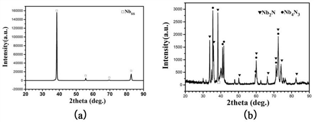
[0086] The surface of the sample before and after nitriding of the niobium-based alloy Nb521 matrix of Example 1 was analyzed by XRD equipment. The XRD pattern is as follows: figure 1 shown. from figure 1 It can be seen from the above that the matrix of the niobium-based alloy Nb521 is a single-phase material, and only the Nbss solid solution phase exists. The nitrided layer formed on the surface of the niobium-based alloy Nb521 after nitriding is mainly Nb 2 N and Nb 4 N 3 Mutually.
[0087] figure 2 The scanning electron microscope image of the cross section of the nitrided layer formed after nitriding the niobium-based alloy Nb521 matrix provided in Example 1 of the present invention. It can be seen from the figure that the thickness of the nitrided layer is uniform and dense, and the bonding with the substrate is good.
[0088] image 3 The macroscopic topography of the surface of the niobium-based alloy Nb521 matrix and the nitrided niobium-based alloy Nb521 provi...
experiment example 2
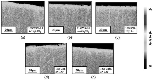
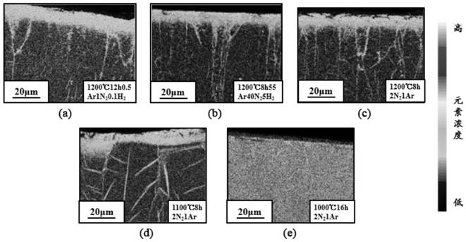
[0092] In order to compare and illustrate the effects of different nitriding process parameters on the properties of the niobium-based alloy after nitriding, the effects of the niobium-based alloy Nb521 after nitriding treatment in Example 1 of the present invention and Comparative Examples 1-4 were tested and compared. The cross-sectional scanning electron microscope backscattering pictures of the 5 groups of niobium-based alloy Nb521 samples after nitriding treatment and the surface distribution maps of Nb and N elements are shown in the following figures, respectively. Figure 6 to Figure 8 shown.
[0093] As can be seen from the figure, the thicknesses of the nitrided layers of Example 1 and Comparative Examples 1 to 4 are 12 to 13 μm, about 10 μm, about 10 μm, about 10 μm, and 6 to 7 μm, respectively.
PUM
| Property | Measurement | Unit |
|---|---|---|
| thickness | aaaaa | aaaaa |
| thickness | aaaaa | aaaaa |
| thickness | aaaaa | aaaaa |
Abstract
Description
Claims
Application Information
 - Generate Ideas
- Intellectual Property
- Life Sciences
- Materials
- Tech Scout
- Unparalleled Data Quality
- Higher Quality Content
- 60% Fewer Hallucinations
Browse by: Latest US Patents, China's latest patents, Technical Efficacy Thesaurus, Application Domain, Technology Topic, Popular Technical Reports.
© 2025 PatSnap. All rights reserved.Legal|Privacy policy|Modern Slavery Act Transparency Statement|Sitemap|About US| Contact US: help@patsnap.com