Preparation method of efficient monocrystalline silicon SE-PERC battery piece

A technology of monocrystalline silicon and solar cells, applied in circuits, photovoltaic power generation, electrical components, etc., can solve the problems of shortened minority carrier diffusion length, dead layer, and photogenerated carriers can no longer be effectively collected, so as to improve conversion efficiency and good rate, the effect of reducing the ratio

Active Publication Date: 2021-04-09
JA SOLAR
View PDF8 Cites 0 Cited by
  • Summary
  • Abstract
  • Description
  • Claims
  • Application Information

AI Technical Summary

Problems solved by technology

[0006] However, as we all know, square resistance and junction depth are a reflection of doping concentration. High square resistance means less doping and shallower junction depth, which will lead to higher Rs and increased contact resistance, which will affect the conversion efficiency of the cell. ;Low square resistance means more doping, deeper junction depth, too much doping will cause dead layer, resulting in a serious decline in passivation quality
During the doping process of gallium-doped silicon wafers, if the doping concentration of the silicon substrate in the base region is increased, it is beneficial to reduce the saturation dark current. However, if the doping concentration is too high, the minority carrier diffusion length will be shortened. When the minority carrier diffusion length When the thickness of the base region is smaller than the thickness of the base region, the photogenerated carriers can no longer be effectively collected, so a compromise doping concentration of the silicon substrate is required. At present, there is no uniform standard for the square resistance of gallium-doped silicon wafers, and the existing shallow junction has high square resistance. The resistivity standard of 0.5-1.5Ω·cm in the diffusion process is only applicable to boron-doped silicon wafers, not to gallium-doped silicon wafers

Method used


Image

  • Preparation method of efficient monocrystalline silicon SE-PERC battery piece
  • Preparation method of efficient monocrystalline silicon SE-PERC battery piece
  • Preparation method of efficient monocrystalline silicon SE-PERC battery piece

Examples


preparation example Construction

[0036] The invention provides a method for preparing a high-efficiency monocrystalline silicon SE-PERC cell, which mainly includes the following steps:

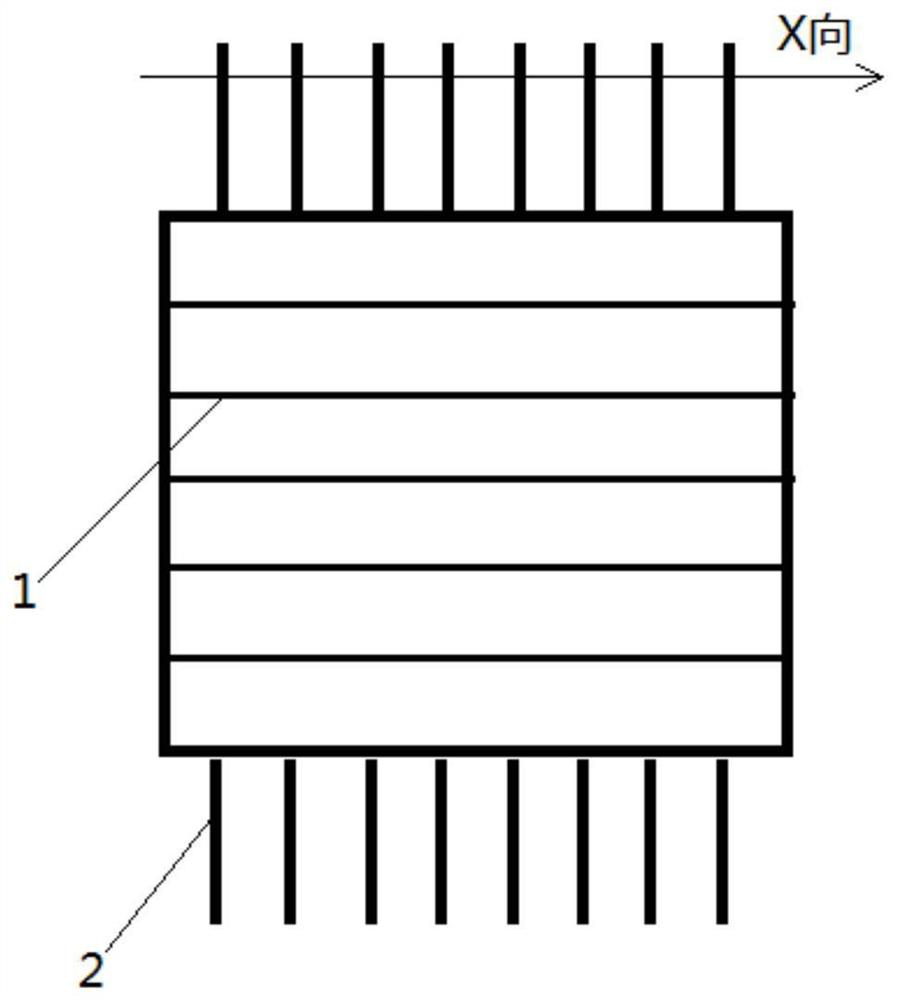
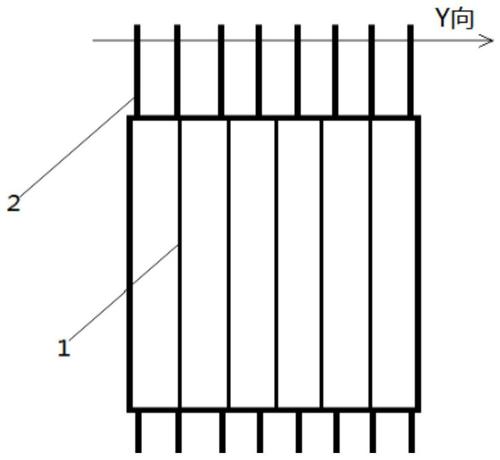
[0037] Select raw silicon wafers: prepare gallium-doped silicon rods, and then cut the gallium-doped silicon rods by wire cutting method to obtain raw silicon wafers, and set the direction of the cutting lines on the silicon wafers as the X direction;

[0038] Texturing: Forming a textured textured surface on the surface of the silicon wafer;

[0039] Diffusion: Phosphorus diffusion treatment is performed on the textured silicon wafer to form a PN junction;

[0040] Laser doping: The diffused silicon wafer is heavily doped with laser, and the graph formed by controlling the laser doping is parallel to the cutting line, that is, it is also in the X direction;

[0041]Phospho-silicate glass removal: remove the phosphorous-silicate glass on the back of the silicon wafer and around it. When removing the phosphorous-silicate glas...

Embodiment 1

[0050] The invention provides a method for preparing a high-efficiency monocrystalline silicon SE-PERC cell, comprising the following steps:

[0051] (1) Step S1, preparing gallium-doped silicon rods, controlling the concentration of gallium elements to ensure that the resistivity is in the range of 0.3-1.1Ω·cm, using diamond wires to cut gallium-doped silicon rods to form X-direction cutting lines Raw silicon wafer;

[0052] (2) Step S2, using a trough type texturing machine to pre-clean and texturize the silicon wafers to ensure that the cutting lines of the silicon wafers in the texturing basket are set vertically;

[0053] (3) Step S3, setting the cutting line direction of the silicon chip after texturing perpendicular to the opening direction of the quartz boat in the diffusion device, forming a PN junction on the surface of the silicon chip after the diffusion step;

[0054] (4) Step S4, according to the metallization pattern of screen printing, the PSG layer formed aft...

Embodiment 2

[0063] The difference from Example 1 is that the passivation film and passivation anti-reflection film on the back of this example are deposited integrally by plate or tube PECVD, and the passivation anti-reflection film is only deposited on the front by tube or plate PECVD.


PUM

PropertyMeasurementUnit
electrical resistivityaaaaaaaaaa

Abstract

The invention discloses a preparation method of an efficient monocrystalline silicon SE-PERC battery piece. The preparation method comprises the steps of raw material silicon wafer selection, texturing, diffusion, laser doping, phosphorosilicate glass removal, passive film deposition, passive antireflection film deposition, back laser grooving, silk-screen printing and sintering. Specifically, the raw material silicon wafer is a silicon wafer prepared through a wire cutting method, cutting lines on the silicon wafer are set to be in the X direction, the conveying direction of the silicon wafer is controlled to be in the Y direction in the phosphorosilicate glass removal step, and an included angle is formed between the Y direction and the X direction. The preparation method provided by the invention can effectively improve the overall conversion efficiency of the battery piece.

Description

technical field [0001] The invention relates to the technical field of production and manufacture of monocrystalline silicon cells, in particular to a method for preparing high-efficiency monocrystalline silicon SE-PERC cells. Background technique [0002] The biggest difference between PERC batteries (Passivated Emitter and Rear Cell) and conventional batteries is that the back surface of the battery is passivated with a dielectric film, and local metal contacts are used to reduce the recombination of the back surface and increase the open circuit voltage. Increase the reflection of the back surface, improve the short-circuit current, and thus improve the efficiency of the battery. Due to its relatively simple process and less cost increase, PERC battery is the mainstream production process at present and in the future. [0003] PERC technology is highly compatible with existing production lines and is easy to upgrade production lines. For example, SE-PERC technology is ba...

Claims


Application Information

Patent Timeline
Patent Type & Authority Applications(China)
IPC IPC(8): H01L31/0236H01L31/0216H01L31/06H01L31/18
CPCH01L31/02363H01L31/02168H01L31/06H01L31/1804H01L31/1868Y02E10/50Y02P70/50Y02E10/547
Inventor 王贵梅张志敏刘苗
Owner JA SOLAR
Why Eureka
Try Eureka