
Chemical vapor deposition method for preparing silicon carbide composite coating on monocrystalline silicon or polycrystalline silicon

A chemical vapor deposition, composite coating technology, applied in the coating, gaseous chemical plating, metal material coating process and other directions, can solve the thermal expansion coefficient mismatch, poor adhesion between the coating and the substrate, etc., to achieve dense structure, Combines well-integrated, smooth-surfaced results

Active Publication Date: 2021-04-13
INST OF METAL RESEARCH - CHINESE ACAD OF SCI
View PDF8 Cites 4 Cited by
  • Summary
  • Abstract
  • Description
  • Claims
  • Application Information

AI Technical Summary

Problems solved by technology

[0006] The purpose of the present invention is to provide a chemical vapor deposition method for preparing a silicon carbide composite coating on single crystal silicon or polycrystalline silicon to solve the problem of poor bonding between the coating and the substrate due to thermal expansion coefficient mismatch

Method used


Image

  • Chemical vapor deposition method for preparing silicon carbide composite coating on monocrystalline silicon or polycrystalline silicon
  • Chemical vapor deposition method for preparing silicon carbide composite coating on monocrystalline silicon or polycrystalline silicon

Examples


Embodiment 1

[0035] In this embodiment, the chemical vapor deposition method for preparing a silicon carbide composite coating on single crystal silicon is as follows:

[0036](1) Ultrasonic cleaning the monocrystalline silicon substrate in deionized water and acetone for 5 minutes, and then cleaning it in hydrofluoric acid with a concentration of 5 wt% for 10 minutes, and placing the silicon substrate in the reaction chamber;

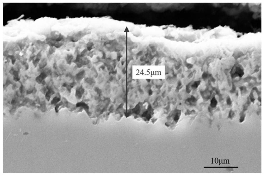
[0037] (2) Prepare a porous silicon layer on the silicon substrate, and pass H 2 and Ar, H 2 The flow rate is 200sccm, the Ar flow rate is 1500sccm, the etching temperature is 1200°C, the working pressure is 200Pa, the etching time is 30min, and the thickness of the porous silicon layer is 24.5μm, see figure 1 ;

[0038] (3) Deposit a very thin SiOC buffer layer on the porous silicon layer, the liquid flow rate of HMDSO is 0.3g / min, H 2 The flows of Ar and Ar are 200sccm and 3000sccm respectively, the deposition temperature is 1050°C, the working pressure is 300...

Embodiment 2

[0044] In this embodiment, the chemical vapor deposition method for preparing a silicon carbide composite coating on polysilicon is as follows:

[0045] (1) Ultrasonic cleaning the polysilicon substrate in deionized water and acetone for 10 minutes, and then cleaning it in hydrofluoric acid with a concentration of 5 wt% for 15 minutes, and placing the silicon substrate in the reaction chamber;

[0046] (2) Prepare a porous silicon layer on the silicon substrate, and pass H 2 and Ar, H 2 The flow rate is 300sccm, the Ar flow rate is 3000sccm, the etching temperature is 1250°C, the working pressure is 400Pa, the etching time is 15min, and the thickness of the porous silicon layer is 12.5μm;

[0047] (3) Deposit a very thin SiOC buffer layer on the porous silicon layer, the liquid flow rate of HMDSO is 0.6g / min, H 2 The flow rates of Ar and Ar are 500sccm and 5000sccm respectively, the deposition temperature is 1100°C, the working pressure is 600Pa, the deposition time is 40min...


PUM

PropertyMeasurementUnit
Thicknessaaaaaaaaaa
Thicknessaaaaaaaaaa
Thicknessaaaaaaaaaa

Abstract

The invention belongs to the field of coating preparation, and particularly relates to a chemical vapor deposition method for preparing a silicon carbide composite coating on monocrystalline silicon or polycrystalline silicon. A metal organic compound chemical vapor deposition (MOCVD) system is adopted, a liquid raw material hexamethyldisilane (HMDS) or hexamethyldisiloxane (HMDSO), H<2> and Ar gas system is selected, the working pressure is 10-1000 Pa, and the temperature is 900-1350 DEG C. Before the coating is deposited, pretreatment is carried out on a monocrystalline silicon or polycrystalline silicon substrate to form a porous silicon layer, then the coating is deposited on the porous silicon layer, and the composite coating sequentially comprises a porous silicon layer, a buffer layer, an SiOC layer and a pure SiC layer from a Si matrix. The silicon carbide composite coating deposited by adopting the method has the advantages of being compact in structure, free of obvious cracks, good in combination with the matrix and the like. According to the composite coating designed by the method, the stress matching problem of the SiC coating and the Si matrix is ingeniously coordinated, and the thickness of the composite coating prepared by adopting the method can exceed 1.5 mm.

Description

technical field [0001] The invention belongs to the technical field of coating preparation, in particular to a chemical vapor deposition method for preparing a silicon carbide composite coating on single crystal silicon or polycrystalline silicon. Background technique [0002] Dry etching is the main technical path for chip manufacturing, commonly used etching gases include SF 6 、CF 4 、C 4 f 8 and O 2 Wait. During the etching process, the main function of the fluorine-containing gas is to obtain fluorine ions through ionization, and the fluorine ions chemically react with the silicon atoms in the silicon carbide substrate to form SiF 4 gas and realize the etching of silicon atoms. At present, since the stage of the silicon wafer is mostly made of silicon material, it is necessary to effectively protect this part of the silicon material in order to improve the service life of the stage. [0003] Silicon carbide material has a large band gap, high breakdown electric fie...

Claims


Application Information

Patent Timeline
IPC IPC(8): C23C16/02C23C16/30C23C16/32
CPCC23C16/0227C23C16/0272C23C16/30C23C16/325
Inventor 唐明强刘厚盛崔新宇王吉强沈艳芳熊天英
Owner INST OF METAL RESEARCH - CHINESE ACAD OF SCI
Learn More