Semiconductor structure and forming method thereof

A semiconductor and graphics layer technology, applied in semiconductor/solid-state device manufacturing, electrical components, circuits, etc., can solve the problems of increasing the difficulty and complexity of integrated circuits, so as to ensure the integrity of graphics, reduce the probability of mis-etching, and improve The effect of craft effect

Pending Publication Date: 2021-04-27
SEMICON MFG INT (SHANGHAI) CORP +1
View PDF0 Cites 3 Cited by
  • Summary
  • Abstract
  • Description
  • Claims
  • Application Information

AI Technical Summary

Problems solved by technology

[0003] During the development of integrated circuits, usually as the functional density (that is, the number of interconnection structures per chip) gradually increases, the geometric size (that is, the minimum component size that can be produced using process steps) also gradually decreases. Correspondingly increases the difficulty and complexity of integrated circuit manufacturing
[0004] At present, in the case of shrinking technology nodes, how to improve the matching degree between the pattern formed on the wafer and the target pattern has become a challenge

Method used


Image

  • Semiconductor structure and forming method thereof
  • Semiconductor structure and forming method thereof
  • Semiconductor structure and forming method thereof

Examples


Embodiment Construction

[0013] At present, the problem of short circuit between interconnect lines formed in the inter-metal dielectric layer is likely to occur. The reasons for the short-circuit problem between interconnect lines are analyzed in combination with a method for forming a semiconductor structure.

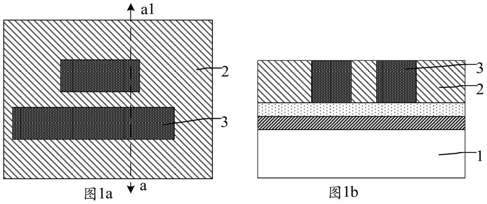
[0014] refer to Figure 1 to Figure 6 , a schematic diagram of the structure corresponding to each step in a method for forming a semiconductor structure is shown.

[0015] refer to figure 1 , figure 1 a is a top view, figure 1 b is figure 1 The cross-sectional view along the secant line aa1 in a, a substrate (not shown) is provided, and a metal interlayer dielectric layer 1 is formed on the substrate.

[0016] continue to refer to figure 1 , a core layer 2 and a plurality of sacrificial layers 3 located in the core layer 2 are formed on the inter-metal dielectric layer 1, and the plurality of sacrificial layers 3 are arranged at intervals.

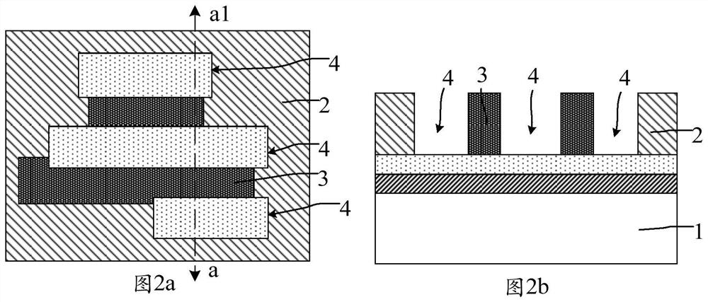
[0017] refer to figure 2 , figure 2...


PUM

PropertyMeasurementUnit
thicknessaaaaaaaaaa

Abstract

The invention discloses a semiconductor structure and a forming method thereof. The forming method comprises the steps of providing a substrate, and forming a to-be-etched layer on the substrate, forming a core layer and a plurality of sacrificial layers located in the core layer on the to-be-etched layer, and enabling the sacrificial layers to be arranged at intervals, removing part of the core layer between the adjacent sacrificial layers to form a first groove penetrating through the core layer, and exposing the sacrificial layers from the side wall of the first groove, carrying out first ion doping treatment on the core layer of the side wall of the first groove, wherein the first ion doping treatment is suitable for increasing the etching resistance of the core layer of the side wall of the first groove, forming a side wall on the side wall of the first groove, after first ion doping processing and side wall forming are carried out, removing the sacrificial layer, forming a second groove penetrating through the core layer, and isolating the second groove and the first groove by a side wall, and etching the to-be-etched layers at the bottoms of the first groove and the second groove by taking the core layer and the side walls as masks. According to the embodiment of the invention, the probability that the core layer on the side wall of the first groove is mistakenly etched in the step of removing the sacrificial layer is reduced.

Description

technical field [0001] Embodiments of the present invention relate to the field of semiconductor manufacturing, and in particular, to a semiconductor structure and a method for forming the same. Background technique [0002] With the rapid growth of the semiconductor integrated circuit (IC) industry, semiconductor technology continues to move towards smaller process nodes driven by Moore's Law, making integrated circuits smaller in size, higher in circuit precision, and in circuits. The direction of higher complexity. [0003] In the development of integrated circuits, as the functional density (ie, the number of interconnect structures per chip) gradually increases, the geometric size (ie, the smallest component size that can be produced by process steps) also gradually decreases. Accordingly, the difficulty and complexity of integrated circuit fabrication are increased. [0004] At present, with the continuous shrinking of technology nodes, how to improve the matching de...

Claims


Application Information

Patent Timeline
Patent Type & Authority Applications(China)
IPC IPC(8): H01L21/311H01L21/768
CPCH01L21/31144H01L21/76802H01L21/76816
Inventor 金吉松窦涛苏波杨明
Owner SEMICON MFG INT (SHANGHAI) CORP
Why Eureka
Try Eureka