Surface pretreatment method of metal material and production process of PCB
A surface pretreatment, metal material technology, applied in the improvement of metal adhesion of insulating substrates, secondary processing of printed circuits, electrical components, etc., can solve problems such as unfavorable high-frequency signal transmission, high-frequency signal attenuation, etc.
- Summary
- Abstract
- Description
- Claims
- Application Information
AI Technical Summary
Problems solved by technology
Method used
Image
Examples
Embodiment 1
[0034] This embodiment provides a method for surface pretreatment of a PCB substrate, the method comprising the following steps:
[0035] S1: Into the board, select the PCB board with copper core board in the inner layer and copper surface after the outer board is electrically or etched, and put it into the pretreatment production line horizontally, and the transmission speed is controlled at 1.5-2.0m / min.
[0036] S2: pickling, pickling with dilute sulfuric acid concentration of 3-6% pickling solution, the control temperature during pickling is 37-43°C, and the control pressure is 0.8-1.8kg / cm 2 .
[0037] S3: One-time washing, using three-stage overflow washing, the volume of each overflow washing tank is 100L, and the washing pressure is controlled at 0.8-1.8kg / cm 2 .
[0038] S4: Bonding agent treatment, under the pH range of 5.5-6.5, the temperature is controlled at 25-28° C., and a bonding agent solution with a concentration of 0.3-0.6 wt% is used to contact the copper...
Embodiment 2
[0044] The present embodiment provides a kind of production technology of PCB board, comprises the following steps:
[0045] Step 1: Use the surface pretreatment method in Example 1 to perform surface pretreatment on the PCB substrate.
[0046]Step 2: use an ink coating wheel to coat a photosensitive ink layer on the surface of the pretreated PCB substrate, and perform baking and drying treatment on the photosensitive ink layer.
[0047] Step 3: Expose the dried PCB substrate to film exposure.
[0048] Step 4: Put the PCB substrate in a developing machine for developing treatment to develop redundant circuits.
[0049] Step 5: After manual visual inspection, place the PCB substrate in an etching machine to etch to remove redundant lines, and finally remove the photosensitive ink layer on the surface, clean and dry.
[0050] Wherein, in the production process of the PCB board, the line types on it may be straight lines, oblique lines, corner lines, arcs and other line types. ...
Embodiment 3
[0052] Comparative Experiment
[0053] The bonding agent solutions with concentrations of 0.1wt%, 0.3wt%, 0.6wt%, and 0.9wt% were used to produce PCB boards by the method in Example 2, and the line width / spacing was set to 70 / 70 μm. Compare the performance of the produced PCB boards, including the following test contents:
[0054] 1. Throwing film inspection: visually inspect the board surface after development, and if there is a flinging film (poor bonding force), it is judged as unqualified;
[0055] 2. AOI scanning: Statistical AOI (automatic optical inspection) scanning defects, the more defect points, the worse the bonding force;
[0056] 3. Line width measurement: After etching, take a slice to measure whether the line width is within the required tolerance range.
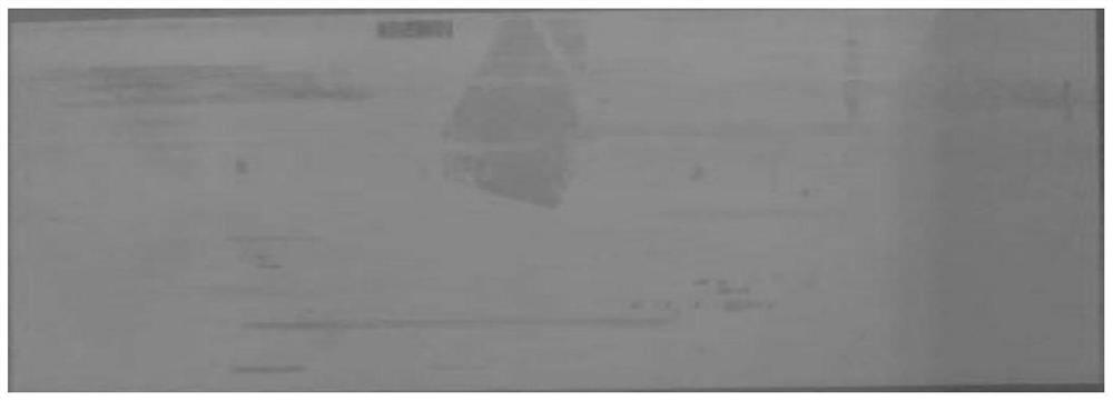
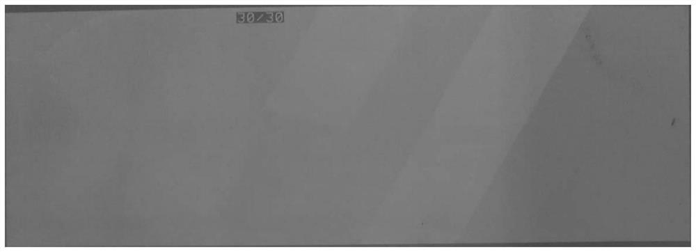
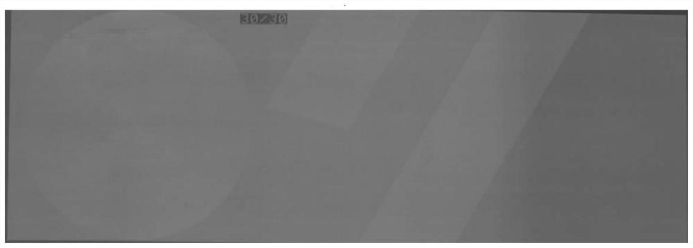
[0057] The film throwing test results are shown in Table 1 and Figure 1~4 , Figure 1 ~ Figure 4 It is the picture of the flung film of the product obtained by pretreating the copper surface when the conc...
PUM
 Abstract
Description
Claims
Application Information


