

Preparation method of semi-insulating silicon carbide single crystal wafer
A silicon carbide single crystal and silicon carbide wafer technology, applied in chemical instruments and methods, single crystal growth, single crystal growth, etc., can solve problems such as low production efficiency, large cooling rate, low concentration, etc., to improve product consistency , the effect of improving performance
- Summary
- Abstract
- Description
- Claims
- Application Information
AI Technical Summary
Problems solved by technology
Method used
Image

Examples
Embodiment Construction
[0023] In order to make the technical problems, technical solutions and beneficial effects to be solved by the present invention clearer, the present invention will be further described in detail in combination with the embodiments and accompanying drawings. It should be understood that the specific embodiments described here are only used to explain the present invention, not to limit the present invention. The technical scheme of the present invention will be described in detail below in conjunction with the embodiments and accompanying drawings, but the scope of protection is not limited thereto.
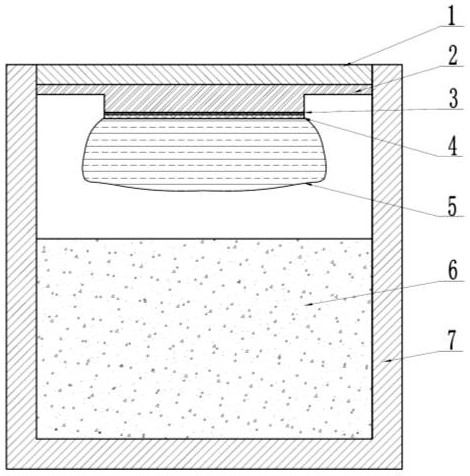
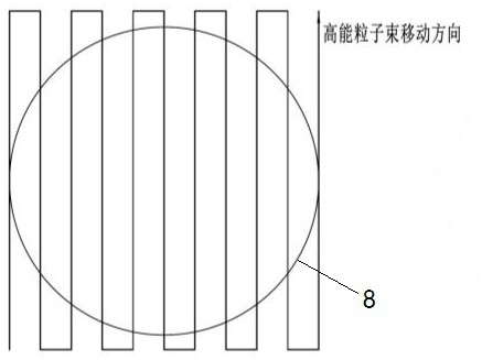
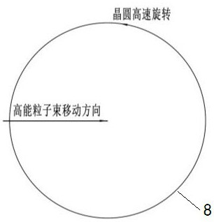
[0024] The invention relates to a method for preparing a semi-insulating silicon carbide single crystal wafer. First, a silicon carbide wafer is prepared, and then high-energy particles are used to irradiate the silicon carbide wafer to introduce point defects into the silicon carbide wafer to compensate for the shallow energy level of the silicon carbide wafer. defect. The spec...
PUM
 Abstract
Description
Claims
Application Information