Tri-gate SiC transverse MOSFET power device

A power device and lateral technology, applied in the field of tri-gate SiC lateral MOSFET power devices, can solve the problems of high threshold voltage, high drive level, and large drive power consumption of SiC power MOSFETs, and achieve low specific on-resistance, current-carrying The effect of increasing sub-concentration and reducing driving energy consumption

Pending Publication Date: 2021-05-07
GLOBAL POWER TECH CO LTD
View PDF0 Cites 0 Cited by
  • Summary
  • Abstract
  • Description
  • Claims
  • Application Information

AI Technical Summary

Problems solved by technology

[0004] The technical problem to be solved by the present invention is to provide a tri-gate SiC lateral MOSFET power device to solve the

Method used


Image

  • Tri-gate SiC transverse MOSFET power device
  • Tri-gate SiC transverse MOSFET power device
  • Tri-gate SiC transverse MOSFET power device

Examples


Embodiment 1

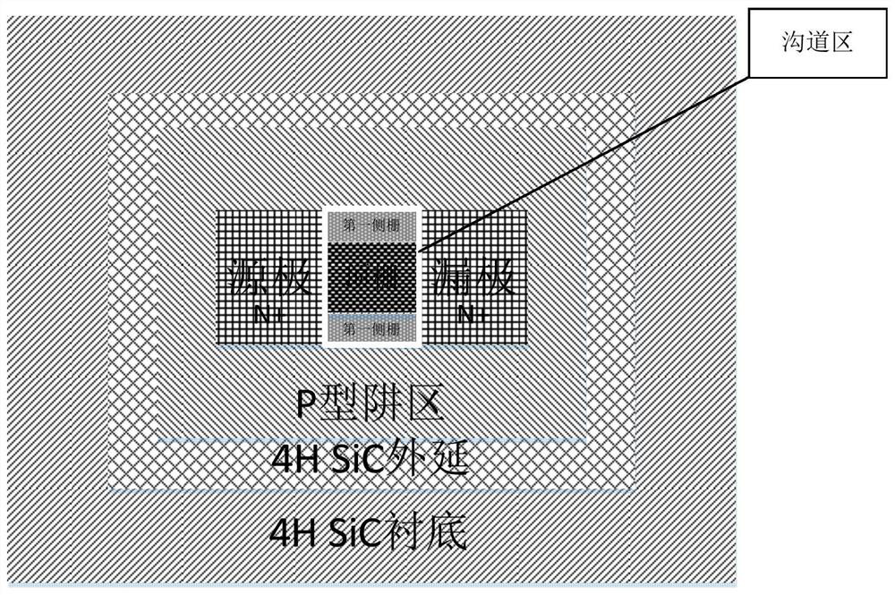
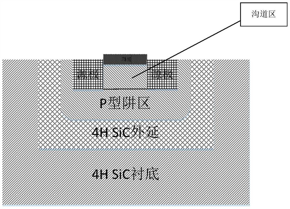
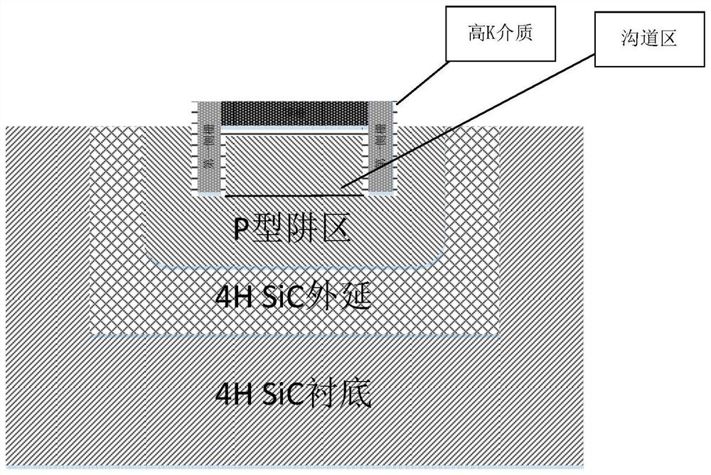
[0027]SeeFigure 1 to 3As shown, this embodiment provides a three-gate SiC lateral MOSFET power device, including

[0028]A SiC substrate is provided with a substrate groove on the SiC substrate;

[0029]A SiC epitaxial layer provided an epitonial groove within the SiC epitaxial layer; the SiC epitaxial layer is disposed within the substrate recess;

[0030]A T-well region is provided with a dielectric groove in which a channel region is provided in which the T-well region is provided in the outer delay groove;

[0031]A gate, the gate comprises two first side grids and a top gate, and the junction of the junction portion is partially connected to the side of the gate of the gate, forming an inverted U-shaped structure, the top gate The first side gate is surrounded by a high K medium, and the down U-shaped structure is provided in the dielectric tank and protrudes in the dielectric tank;

[0032]A drain, the source is housed in the dielectric tank and is provided on one side of the U-shaped struct...

Embodiment 2

[0042]Such asFigure 4 As shown, based on the first example, a multi-gate structure, that is, two first side grids, at least one second side gate, further reduce the threshold voltage, and improve the capacity.


PUM


Abstract

The invention provides a tri-gate SiC transverse MOSFET power device. The device comprises a SiC substrate, a SiC epitaxial layer, a P-type well region, a grid electrode, a drain electrode and a source electrode;a substrate groove is formed in the SiC substrate; an epitaxial groove is formed inthe SiC epitaxial layer; the SiC epitaxial layer is arranged in the substrate groove; the P-type well region is provided with a medium groove, and a channel region is arranged in the medium groove; the P-type well region is arranged in the epitaxial groove; the grid electrode comprises two first side grids and a top grid; the two end parts of the top grid are respectively connected to the side surface of one end part of the grid electrode to form an inverted U-shaped structure, the top grid and the first side grids are surrounded by high-k dielectric except the tops and the connecting part of the top grid and the first side grids, and the inverted U-shaped structure is arranged in the dielectric groove and protrudes out of the dielectric groove; and the drain electrode and the source electrode are arranged in the medium groove and are arranged on the two sides of the U-shaped structure. The problems that the SiC power MOSFET is high in threshold voltage, high in driving level during saturation work and large in driving power consumption are solved.

Description

Technical field[0001]The present invention relates to a three-gate SiC lateral MOSFET power device.Background technique[0002]Sic silicon carbide (SiC) materials are widely received and studied because of their superior physical properties. Its high-temperature power electronics have the advantages of high input impedance, fast switching speed, high operating frequency, high temperature resistance and high pressure, have made widespread use in switching regulator power, high frequency heating, automotive electronics, and power amplifiers.[0003]However, there is still a threshold voltage high, the driving voltage is high, and the material defect is much reduction, the channel mobility is low, the cost is higher, and the economic problem has caused serious restrictions on the development of SiC power devices.Inventive content[0004]The technical problem to be solved by the present invention is to provide a problem of three grid SiC lateral MOSFET power devices, solving the SiC power MOS...

Claims


Application Information

Patent Timeline
IPC IPC(8): H01L29/78H01L29/06H01L29/10H01L29/16H01L29/423
CPCH01L29/0607H01L29/0684H01L29/1033H01L29/1608H01L29/42356H01L29/4236H01L29/7831
Inventor 施广彦秋琪李昀佶
Owner GLOBAL POWER TECH CO LTD
Why Eureka
Try Eureka