Silicon oxide passivation PERC double-sided battery and preparation method thereof
A double-sided battery and silicon oxide technology, which is applied in circuits, photovoltaic power generation, electrical components, etc., can solve the problems of increasing battery manufacturing costs, not conforming to the development trend of cost reduction in the photovoltaic industry, grid parity, and poor anti-PID performance
- Summary
- Abstract
- Description
- Claims
- Application Information
AI Technical Summary
Problems solved by technology
Method used
Image
Examples
Embodiment 1
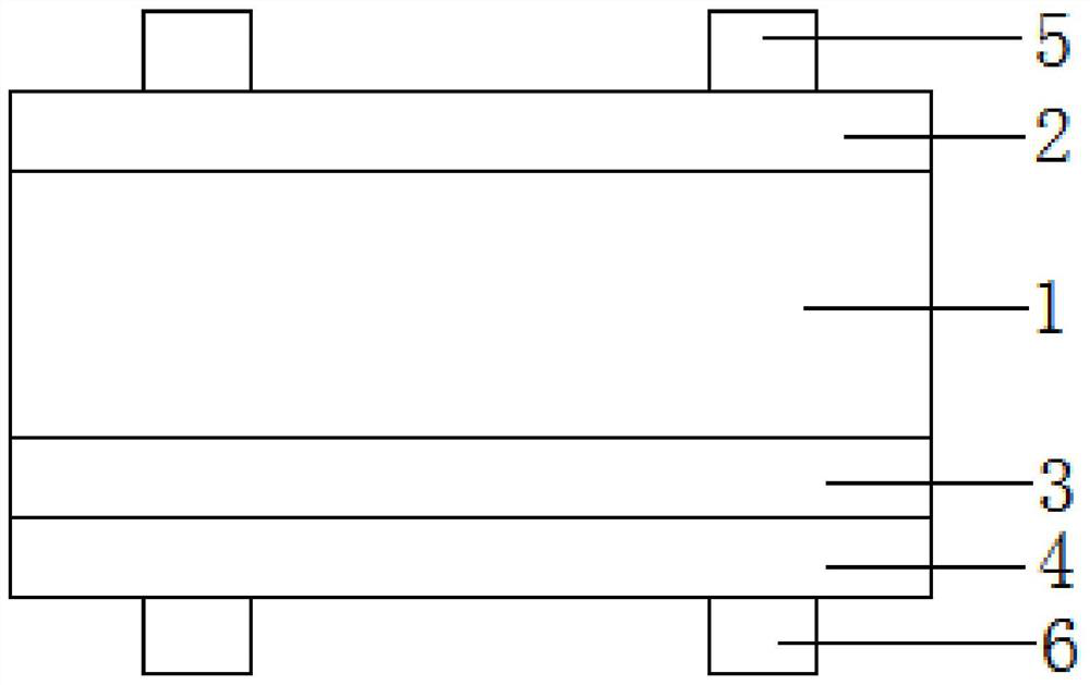
[0031] A silicon oxide passivated PERC double-sided cell, comprising a silicon substrate 1, a front dielectric layer 2 deposited on the front side of the silicon substrate 1, a first dielectric layer 3 deposited on the back side of the silicon substrate 1 and The second dielectric layer 4 deposited on the first dielectric layer 3; the front dielectric layer 2 includes a silicon dioxide layer and a silicon nitride layer; the first dielectric layer 3 is oxynitride Silicon layer, and the thickness of silicon oxynitride layer is 15nm; Described second dielectric layer 4 comprises two layers of silicon nitride layers, and the comprehensive thickness of two layers of silicon nitride layers is 90nm; The first layer of silicon nitride layer The thickness is 40nm, and the thickness of the second silicon nitride layer is 50nm.
[0032] The preparation method of the silicon oxide passivated PERC double-sided battery of the above-mentioned embodiment 1 includes the following specific step...
Embodiment 2
[0043] A silicon oxide passivated PERC double-sided cell, comprising a silicon substrate 1, a front dielectric layer 2 deposited on the front side of the silicon substrate 1, a first dielectric layer 3 deposited on the back side of the silicon substrate 1 and The second dielectric layer 4 deposited on the first dielectric layer 3; the front dielectric layer 2 includes a silicon dioxide layer and a silicon nitride layer; the first dielectric layer 3 is oxynitride Silicon layer, and the thickness of silicon oxynitride layer is 30nm; Described second dielectric layer 4 comprises two layers of silicon nitride layers, and the comprehensive thickness of two layers of silicon nitride layers is 110nm; The first layer of silicon nitride layer The thickness is 50nm, and the thickness of the second silicon nitride layer is 60nm.
[0044] The preparation method of the silicon oxide passivated PERC double-sided battery of the above-mentioned embodiment 2 includes the following specific ste...
Embodiment 3
[0055] A silicon oxide passivated PERC double-sided cell, comprising a silicon substrate 1, a front dielectric layer 2 deposited on the front side of the silicon substrate 1, a first dielectric layer 3 deposited on the back side of the silicon substrate 1 and The second dielectric layer 4 deposited on the first dielectric layer 3; the front dielectric layer 2 includes a silicon dioxide layer and a silicon nitride layer; the first dielectric layer 3 is silicon oxide layer, and the thickness of the silicon oxide layer is 20nm; the second dielectric layer 4 is two silicon nitride layers, and the combined thickness of the two silicon nitride layers is 80nm, the thickness of the first silicon nitride layer is 40nm; the thickness of the second silicon nitride layer is 40nm.
[0056] The preparation method of the silicon oxide passivated PERC double-sided battery of the above-mentioned embodiment 3 includes the following specific steps:
[0057] S1. Pre-cleaning and texturing of the...
PUM
| Property | Measurement | Unit |
|---|---|---|
| thickness | aaaaa | aaaaa |
| thickness | aaaaa | aaaaa |
| thickness | aaaaa | aaaaa |
Abstract
Description
Claims
Application Information
