Preparation method of OLED display screen

A technology for display screens and pixels, which is applied in semiconductor/solid-state device manufacturing, semiconductor devices, electrical components, etc., and can solve problems such as device leakage current, difficulty in controlling the light-emitting area, and uneven light emission.

Active Publication Date: 2021-05-11
SOUTH CHINA UNIV OF TECH
View PDF9 Cites 0 Cited by
  • Summary
  • Abstract
  • Description
  • Claims
  • Application Information

AI Technical Summary

Problems solved by technology

When the pixel size is relatively large, the edge electric field and the electric field intensity in the middle of the electrode are obviously different, and the material diffusion at the edge will add new radial diffusion in addition to the vertical axial diffusion, resulting in poor film quality at the edge and luminescence. The efficiency is low, and the electroluminescent area of ​​the pixel is difficult to control, which may easily lead to problems such as leakage current, uneven light emission and even short circuit of the device.

Method used


Image

  • Preparation method of OLED display screen
  • Preparation method of OLED display screen
  • Preparation method of OLED display screen

Examples


Embodiment 1

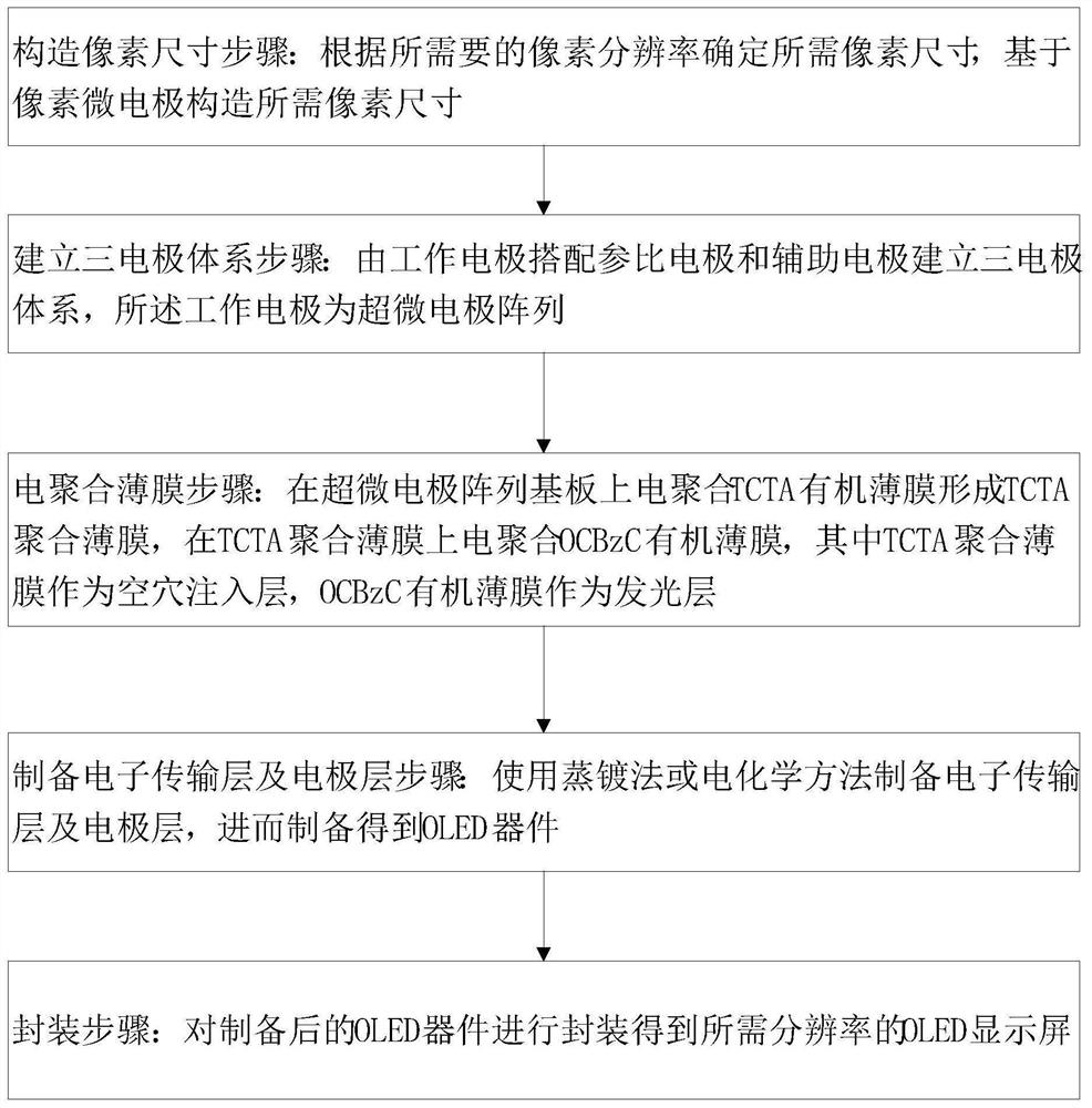
[0046] Such as figure 1As shown, the present embodiment provides a method for preparing an OLED display, the method comprising the following steps:

[0047] Constructing the pixel size step: determining the required pixel size according to the required pixel resolution, and constructing the required pixel size based on the pixel microelectrode;

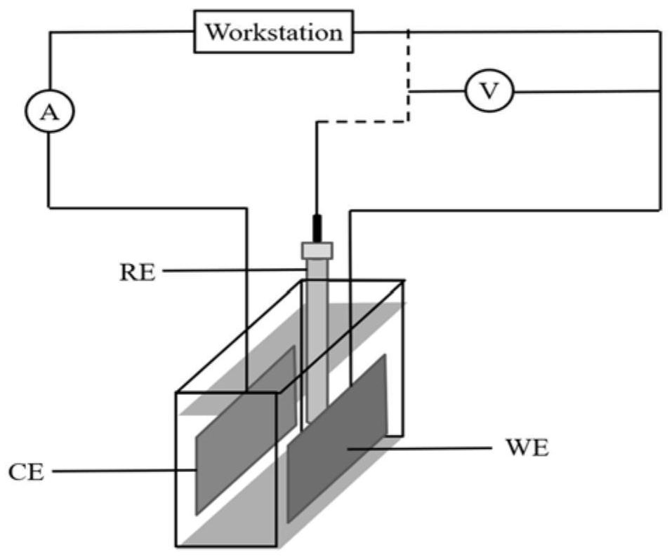
[0048] Steps to establish a three-electrode system: a three-electrode system is established by using a working electrode (WE) with a reference electrode (RE) and an auxiliary electrode (CE), in which the working electrode is an ultramicro electrode array;

[0049] Electropolymerization film step: electropolymerize TCTA organic film on the ultra-micro electrode array substrate to form TCTA polymer film, and electropolymerize OCBzC organic film on the TCTA polymer film, wherein the TCTA polymer film is used as the hole injection layer, and the OCBzC organic film is used as the light emitting layer;

[0050] The step of preparing the el...

Embodiment 2

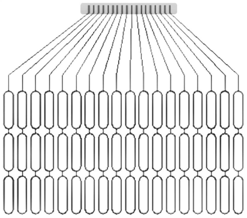
[0080]In this embodiment, a further improvement is made in the step of constructing the pixel size in the method for preparing the OLED display screen proposed in Embodiment 1. Based on the pixel microelectrodes in Embodiment 1, this embodiment uses a preset number of pixel microelectrodes as pixels The primitives form a complex pixel structure, that is, multiple pixel microelectrodes are connected in an array to form a parallel strip structure, and are arranged to form a pixel primitive. The size of the pixel primitive is the required pixel size, and multiple pixel primitives follow the Arranging at equal intervals, and then preparing OLED display screens, since the remaining steps have not been improved, details will not be repeated here.

[0081] In this embodiment, taking a pixel microelectrode with a size of 4 μm×12 μm as an example, the pixel microelectrode is used as a pixel unit to design different pixel sizes, so as to obtain a substrate with the required resolution; i...


PUM

PropertyMeasurementUnit
sizeaaaaaaaaaa
thicknessaaaaaaaaaa
surface roughnessaaaaaaaaaa

Abstract

The invention discloses a preparation method of an OLED display screen. The method comprises the following steps: constructing a pixel size: determining the required pixel size according to the required pixel resolution, and constructing the required pixel size based on a pixel microelectrode; establishing a three-electrode system: establishing the three-electrode system by matching a working electrode with a reference electrode and an auxiliary electrode, wherein the working electrode is an ultramicro electrode array; carrying out a thin film electro-polymerization step: electro-polymerizing a TCTA organic thin film on the ultramicro electrode array substrate to form a TCTA polymerized thin film, and electro-polymerizing an OCBzC organic thin film on the TCTA polymerized thin film; preparing an electron transport layer and an electrode layer: preparing the electron transport layer and the electrode layer by using an evaporation method, and further preparing an OLED device; and packaging: packaging the prepared OLED device to obtain the OLED display screen with the required resolution. According to the method, electrochemical deposition and an ultramicro electrode are combined, and the size of an electro-polymerization pixel is selected according to the actual pixel size, so that the electrochemical method is applicable to preparation of display screens with different resolutions.

Description

technical field [0001] The invention belongs to the technical field of OLED production, in particular to a method for preparing an OLED display screen. Background technique [0002] Resolution is one of the important performance indicators of a display, and different resolutions are usually selected under different usage environments and usage distances. Different resolutions correspond to different pixel sizes, pixel pitches, and pixel densities. A display method is usually suitable for a part of the pixel size. Different resolutions require different display methods. [0003] Electrochemical deposition technology is a method of forming a polymer film on the electrode by using electroactive monomers to undergo oxidation or reduction coupling reactions at the contact interface between the electrode and the solution. , Aggregation structure and other properties can be precisely regulated through the selection of electrochemical deposition methods and conditions. Electrochemi...

Claims


Application Information

Patent Timeline
Patent Type & Authority Applications(China)
IPC IPC(8): H01L51/56H01L27/32
CPCH10K71/125H10K71/164H10K71/60H10K59/12H10K59/1201H10K71/00
Inventor 刘琳琳陈志华梁依倩
Owner SOUTH CHINA UNIV OF TECH
Why Eureka
Try Eureka