High-dielectric grain boundary layer ceramic material and preparation method of grain boundary layer ceramic substrate

A ceramic material and high mesogen technology, applied in the field of capacitors, can solve problems such as poor product performance stability, cracking, and easy curling of ceramic substrates

Active Publication Date: 2021-05-18
BEIJING YUANLIU HONGYUAN ELECTRONICS TECH +2
View PDF11 Cites 2 Cited by
  • Summary
  • Abstract
  • Description
  • Claims
  • Application Information

AI Technical Summary

Problems solved by technology

[0004] In terms of technology, there are two preparation methods for the preparation of grain boundary layer ceramic substrates: primary sintering and secondary sintering; The reduction and oxidation reactions are completed successively during the heating and cooling process, the process control is difficult, and the product performance stability is poor; the commercially available products are mainly secondary sintering, first high-temperature reduction sintering, and then oxidation heat treatment in the air, the product performance is relatively low. Stable and high reliability, but the reduction and sintering temperature is too high (about 1450°C)
[0005] In summary, the main problems in the preparation of high-mesogenic boundary layer ceramic substrates are the high reduction and sintering temperature, the ceramic substrate is easy to curl, crack, and poor insulation performance; the final product performance consistency, low reliability

Method used


Image

  • High-dielectric grain boundary layer ceramic material and preparation method of grain boundary layer ceramic substrate
  • High-dielectric grain boundary layer ceramic material and preparation method of grain boundary layer ceramic substrate
  • High-dielectric grain boundary layer ceramic material and preparation method of grain boundary layer ceramic substrate

Examples


preparation example Construction

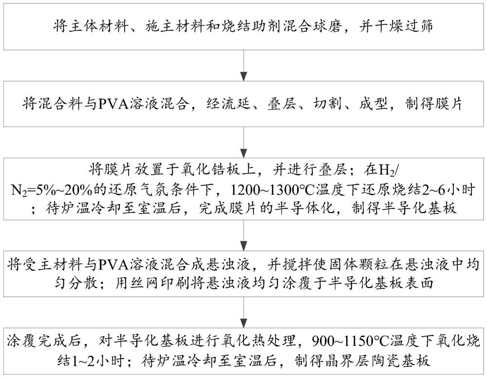
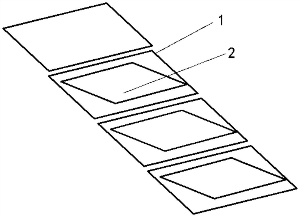
[0066] Such as figure 1 As shown, the present invention provides a method for preparing a ceramic substrate with a high-mesogenic grain boundary layer, which completes the preparation of a ceramic substrate with a grain boundary layer by secondary lamination and sintering, which are respectively reducing semiconductor sintering and oxidizing grain boundary layer insulation sintering, specifically including:

[0067] Step 1, mixing and ball-milling the main material, the donor material and the sintering aid, drying and sieving to prepare the mixture;

[0068] Specifically:

[0069] The strontium titanate main material and La 2 o 3 , Nb 2 o 5 , SiO 2 , Li 2 CO 3 Add it into the ball mill, mix and ball mill for 5-8 hours, dry the material after discharge, and pass through a 60-mesh sieve to obtain a particle size of d 50 <3μm mixture.

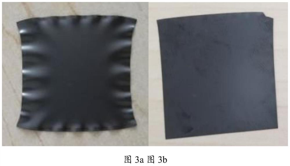
[0070] Step 2, mixing the mixture with the PVA solution, and then casting, laminating, cutting, and forming to obtain a membrane;

[00...

Embodiment

[0083] The present invention provides a high-mesogenic boundary layer ceramic material. The formula of the reduced sintered material is shown in Table 1, and the formula of the oxidized sintered coating material is shown in Table 2, and the unit is g:

[0084] Table 1

[0085] Sample serial number 1 2 3 4 5 6 SrTiO 3

900 900 900 900 900 900 La 2 o 3

3.3 3.3 3.3 3.3 3.3 3.3 Nb 2 o 5

4 4 4 4 4 4 Li 2 CO 3

/ 9.2 9.2 9.2 9.2 9.2 SiO 2

/ / 1.8 1.8 1.8 1.8 Sintering temperature 1450℃ 1250℃ 1250℃ 1250℃ 1250℃ 1250℃

[0086] Table 2

[0087]

[0088] The present invention provides a method for preparing a grain boundary layer ceramic substrate based on the ceramic material of the above-mentioned samples 1-6, comprising:

[0089] Step 1. Weigh the material with corresponding quality according to the formula in Table 1, grind it on a ball mill for 5 hours, discharge, dry, a...


PUM

PropertyMeasurementUnit
sizeaaaaaaaaaa

Abstract

The invention discloses a high-dielectric grain boundary layer ceramic material and a preparation method of a grain boundary layer ceramic substrate. The ceramic material comprises a main body material strontium titanate, a donor materials La2O3 and Nb2O5, a sintering aid SiO2 and Li2CO3, and an acceptor material which is one or more of Bi2O3, CuO and ZnO; the sintering aid is used for reducing the sintering temperature of the ceramic and promoting crystal grain development; and the acceptor material is used as a grain boundary insulation coating material for oxidation sintering. Based on the ceramic material, the preparation of the grain boundary layer ceramic substrate is completed through secondary sintering, namely reduction semiconductor sintering and oxidation grain boundary layer insulation sintering. The ceramic substrate is prepared by doping the sintering aid into the ceramic material and adopting a secondary sintering mode, so that on one hand, the energy is saved, and on the other hand, the larger particle size can be obtained at a lower sintering temperature, and the dielectric constant is favorably improved; and meanwhile, in the grain boundary insulation process, ZnO is added, and the insulation resistance and the insulation strength of the product are improved.

Description

technical field [0001] The invention relates to the technical field of capacitors, in particular to a high-medium grain boundary layer ceramic material and a preparation method of a grain boundary layer ceramic substrate. Background technique [0002] The miniaturization trend of electronic devices requires capacitors to have smaller dimensions and greater energy storage density, and grain boundary layer ceramics have ultra-high dielectric constants, which meet the requirements of capacitors, and are therefore widely used as dielectric materials for capacitors. [0003] At present, there is still a large gap between domestic R&D and mass production capacity of grain boundary layer ceramic materials with high dielectric constant and similar foreign products. The dielectric constant of foreign related ceramics can reach 10,000-60,000 and has been mass-produced; while domestic similar products are reliable. There is a certain gap between foreign countries in terms of performanc...

Claims


Application Information

Patent Timeline
Patent Type & Authority Applications(China)
IPC IPC(8): C04B35/47C04B35/622C04B35/64C04B41/87
CPCC04B35/47C04B35/622C04B35/64C04B41/50C04B41/5074C04B41/87C04B2235/3227C04B2235/3251C04B2235/3418C04B2235/442C04B2235/3298C04B2235/3284C04B2235/3281C04B41/5072C04B41/5049
Inventor 杜君程华容王新祁晓旭赵伟利王帅
Owner BEIJING YUANLIU HONGYUAN ELECTRONICS TECH
Why Eureka
Try Eureka