

Lunar dust protection conductive film with micro-nano structure and preparation method thereof
A technology of micro-nano structure and conductive film, applied to the conductive layer on the insulating carrier, equipment for manufacturing conductive/semiconductive layer, cable/conductor manufacturing, etc., to achieve good moon dust protection effect, good conductive properties, good Effects of Lunar Environmental Adaptability
- Summary
- Abstract
- Description
- Claims
- Application Information
AI Technical Summary
Problems solved by technology
Method used
Image

Examples
Embodiment 1-5
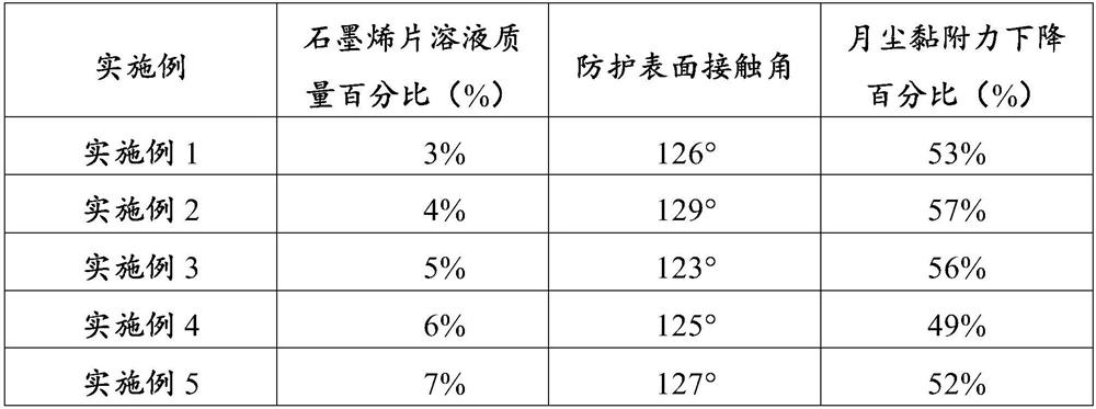
[0034] Embodiment 1-5: Secondary nano conductive filling layer 3 solvent ratio
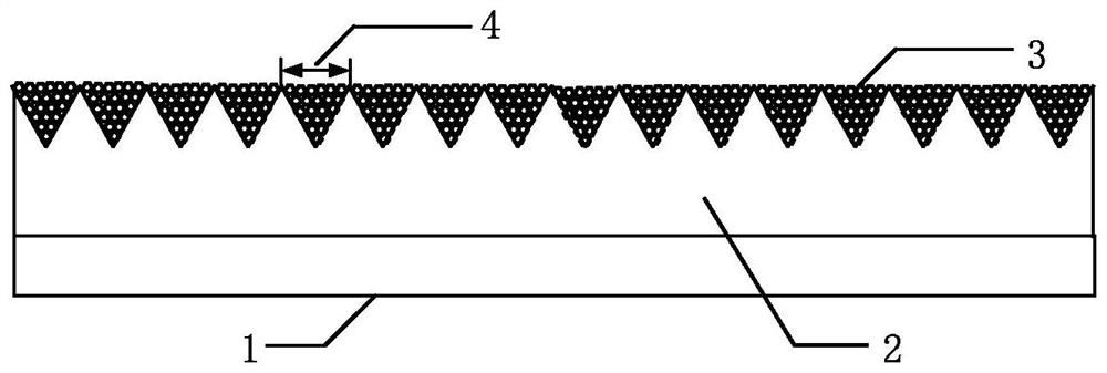
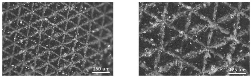
[0035] The aluminum metal substrate was ultrasonically cleaned with ethanol and ultrapure water for 15 minutes in turn for surface polishing treatment, and then placed in a plasma treatment box for plasma treatment (power 200w, time 30s), and the surface polishing treatment of aluminum Coat a layer of 3M 2216 B / A gray glue on the metal substrate, then spin-coat ITO aqueous solution (5000r / min, 10s), then place it in an oven to dry for 30min (70°C), take it out and perform compression molding, and then put it in the oven to dry 4h (70°C). On the surface of the primary micron structure layer 2, evenly spray the graphene sheet solution with a mass fraction of 3%, 4%, 5%, 6% and 7%, spray for 10s, then place it in an oven at 70°C for 0.5h, and take it out Afterwards, evenly wipe off the graphene sheet solution that is not closely adhered to the surface to form a secondary nanometer conductive filling...
Embodiment 6-10
[0039] Embodiment 6-10: Secondary nano conductive filling layer 3 solvent ratio
[0040] Complete the preparation of the first-level micron structure of the film according to the method steps listed in Examples 1-5. The second-level nano-conductive filling layer 3 is sprayed with carbon nanotube solutions with different mass fractions, sprayed for 10 seconds, and then placed in an oven at 70 ° C. Bake for 0.5h, take it out and evenly wipe off the carbon nanotube solution that is not tightly bonded on the surface to form a secondary nano-conductive filling layer 3. The contact angle of the protective film and the decrease in the adhesion of moon dust measured through experiments are shown in Table 2. .
[0041] Table 2 Performance comparison under different carbon nanotube concentrations
[0042]
[0043] The study found that the mass percentage of the carbon nanotube solution directly affects the contact angle of the protective conductive film and the adhesion force with t...
Embodiment 11-13
[0044] Examples 11-13: Secondary nanometer conductive filling layer 3 solvent ratio
[0045] Complete the preparation of the first-level micron structure of the film according to the method steps listed in Examples 6-9. The second-level nano-conductive filling layer 3 is sprayed with white carbon black solutions with different mass fractions, sprayed for 10 seconds, and then placed in an oven at 70 ° C. Bake for 0.5h, take it out and evenly wipe off the silica solution that is not tightly bonded on the surface to form a second-level nano-conductive filling layer 3. The contact angle of the protective film and the decrease in the adhesion of moon dust measured through experiments are shown in Table 3. .
[0046] Table 3 Performance comparison under different silica concentrations
[0047]
[0048] The study found that the mass percentage of silica solution directly affects the contact angle of the protective conductive film and the adhesion between the protective conductive...
PUM
 Abstract
Description
Claims
Application Information