Preparation method of transistor channel, source electrode and drain electrode based on micro-region electrochemical etching

A source-drain electrode, electrochemical technology, used in transistors, semiconductor/solid-state device manufacturing, circuits, etc., can solve the problems of complex process, high cost, low resolution, etc., and achieve the effect of solving complex process

Inactive Publication Date: 2021-06-01
FUDAN UNIV +1
View PDF6 Cites 1 Cited by
  • Summary
  • Abstract
  • Description
  • Claims
  • Application Information

AI Technical Summary

Problems solved by technology

[0003] The purpose of the present invention is to provide a method for preparing transistor channel and source-drain electrodes based on micro-area electrochemical etching, so as to effectively solve the problems of complex process, high cost or low resolution in the manufacture of existing mask electrodes

Method used


Image

  • Preparation method of transistor channel, source electrode and drain electrode based on micro-region electrochemical etching
  • Preparation method of transistor channel, source electrode and drain electrode based on micro-region electrochemical etching
  • Preparation method of transistor channel, source electrode and drain electrode based on micro-region electrochemical etching

Examples


Embodiment 1

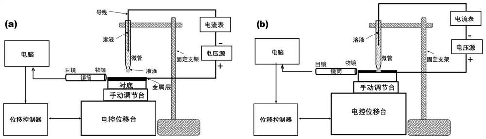
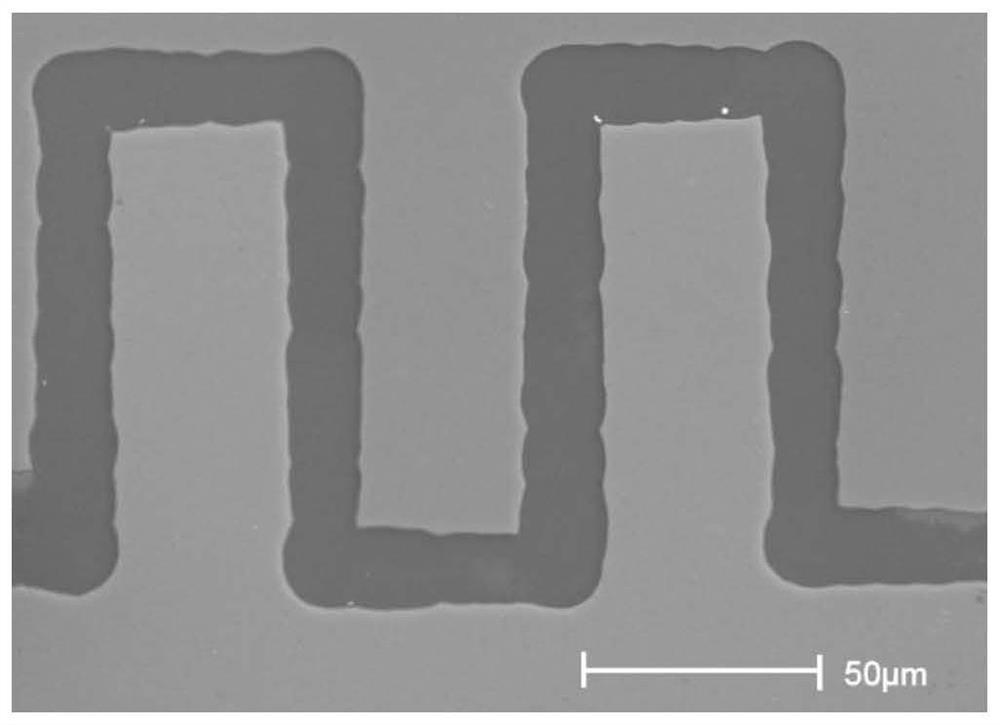
[0029] In this example, SiO 2 Taking the preparation of inter-finger electrodes on the / Si substrate as an example, the preparation method of transistor channel and source-drain electrodes based on micro-area electrochemical etching in the present invention is explained. The microtube used is a glass capillary treated by heating and stretching, and the diameter of the tip of the capillary is 15 microns. 0.5M CuSO 4 As an electrolyte, insert a copper wire into the electrolyte to ground. SiO 2 A copper layer with a thickness of 85 nanometers is deposited on the / Si substrate by vacuum thermal evaporation process, and a bias voltage of 2V is applied to the copper layer. Fill the prepared microtubes with 0.5M CuSO 4 . Fix the glass microtube above the substrate, and use the electric translation stage to control the upward movement of the substrate until it is observed that the electrolyte forms a liquid meniscus between the nozzle of the glass microtube and the substrate and ...

Embodiment 2

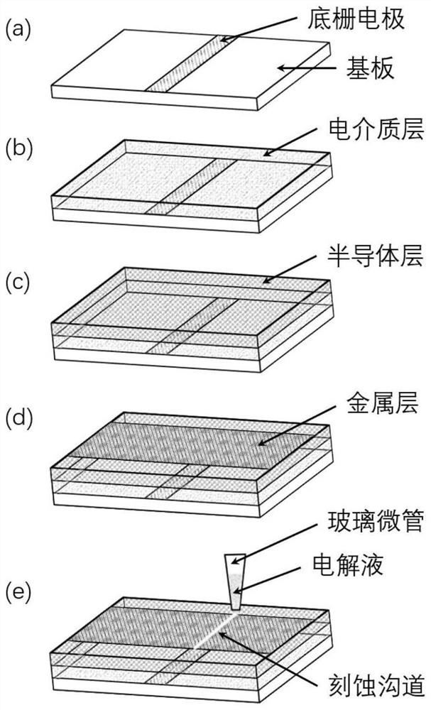
[0032] This example takes the preparation of bottom-gate top-contact structure transistors on flexible polyimide substrates as an example, and explains the method for preparing transistor channels and source-drain electrodes based on micro-area electrochemical etching in the present invention. The specific steps as follows:

[0033] Step 1: prepare an aluminum bottom gate electrode with a width of 1mm and a thickness of 50nm by vacuum deposition on the cleaned polyimide substrate;

[0034] Step 2: Prepare a PVDF-TrFE-CTFE dielectric layer on the aluminum electrode described in Step 1 by spin coating, and anneal at 130° C. for 3 hours;

[0035] Step 3: Prepare organic semiconductor DPP-DTT on the dielectric layer described in Step 2 by spin coating, and anneal at 130° C. for 3 hours;

[0036] Step 4: Prepare copper stripes with a width of 0.78 mm and a thickness of 85 nm by vacuum deposition on the organic semiconductor layer described in step 3;

[0037] Step five: use the m...


PUM

PropertyMeasurementUnit
diameteraaaaaaaaaa
diameteraaaaaaaaaa

Abstract

The invention belongs to the field of preparation of electronic devices, and particularly relates to a preparation method of a transistor channel, a source electrode and a drain electrode based on micro-region electrochemical etching. According to the method, an electrochemical principle and a micro-area self-confinement processing technology are combined, specifically, a meniscus is formed in a specific area of a substrate by using a microtube filled with electrolyte, and a patterned electrode is prepared by applying voltage between the electrolyte and a conductive metal layer of the substrate and enabling a needle tube to move relative to the substrate according to a planned path and speed. By efficiently and flexibly controlling the micro-region electrochemical etching of the metal material, the problems of complex process, high cost or low resolution in the existing mask electrode manufacturing process (such as photoetching and vacuum evaporation) are effectively solved. The method has important significance on laboratory research and industrial production.

Description

technical field [0001] The invention belongs to the field of electronic device preparation, and in particular relates to a method for preparing a transistor channel and source-drain electrodes. Background technique [0002] Metal electrode micropatterns are an important part of electronic devices such as field-effect transistors, where the shape and size control of the channel between the source and drain of the transistor is the key to the fabrication technology. Photolithography is the most commonly used electrode preparation technology at present, but it needs to customize a variety of masks to realize the manufacture of different electrode patterns, which has limitations such as complex operation and expensive equipment. Vacuum deposition, which is commonly used in the preparation of laboratory electrode patterns, also requires the use of masks, and generally has a low resolution, which makes it difficult to meet the accuracy requirements. In addition, due to the high s...

Claims


Application Information

Patent Timeline
Patent Type & Authority Applications(China)
IPC IPC(8): H01L21/306H01L21/336H01L29/40H01L29/417H01L29/10
CPCH01L21/30604H01L29/66477H01L29/401H01L29/41725H01L29/1029
Inventor 朱国栋王丛欢陶鑫
Owner FUDAN UNIV
Why Eureka
Try Eureka