Contact vibration photon sensor utilizing Doppler effect and manufacturing method thereof

A technology of photon sensor and Doppler effect, applied in the direction of using wave/particle radiation, semiconductor/solid-state device manufacturing, and technology for producing decorative surface effects, etc., can solve speckle noise, large environmental impact, and difficulty in measuring laser reflection Insensitive to objects and other issues, to achieve high-precision results

Active Publication Date: 2021-07-20
OTN INTELLIGENT TECH (SUZHOU) CO LTD
View PDF8 Cites 0 Cited by
  • Summary
  • Abstract
  • Description
  • Claims
  • Application Information

AI Technical Summary

Problems solved by technology

However, there are still some shortcomings in this technology that have not been overcome, such as speckle noise, difficulty in measuring objects that are not sensitive to laser reflection, and a section of the optical path exposed to the external environment, which is greatly affected by the environment.

Method used


Image

  • Contact vibration photon sensor utilizing Doppler effect and manufacturing method thereof
  • Contact vibration photon sensor utilizing Doppler effect and manufacturing method thereof
  • Contact vibration photon sensor utilizing Doppler effect and manufacturing method thereof

Examples


Embodiment 1

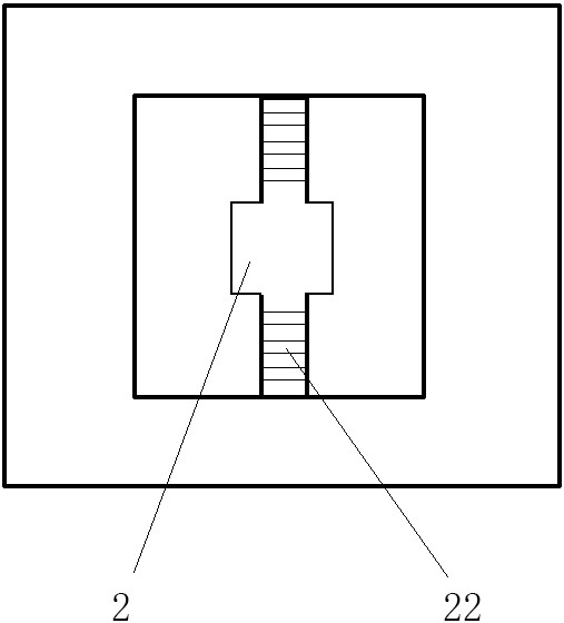
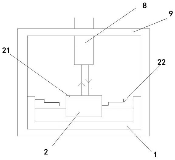
[0064] This embodiment provides a contact vibration photon sensor utilizing the Doppler effect, including an outer packaging layer 9, such as figure 1 As shown, the outer encapsulation layer 9 also includes:

[0065] Silicon-based material 1, comprising a side wall 10 and a cavity 11 surrounded by the side wall 10 with an open top;

[0066] The mirror body 2 is arranged in the cavity 11, the top of the mirror body 2 has a mirror layer 21, the side of the mirror body 2 is connected with the side wall 10 by a cantilever beam 22, and the cantilever beam 22 is a spring shape ( That is to say, the cantilever beam 22 has grooves perpendicular to the mirror layer 21 with different opening directions, and the projections of the two kinds of grooves on the plane where the mirror layer 21 is located are arranged in a dislocation).

[0067] The shape of the mirror body 2 can be a cube, or a cylinder with at least two parallel sides.

[0068] When the mirror body 2 is cube-shaped, such ...

Embodiment 2

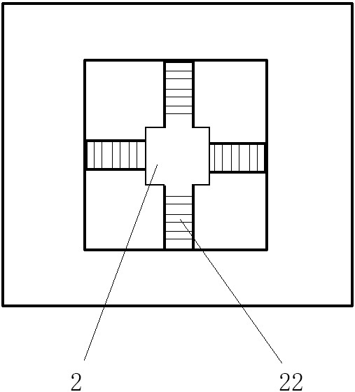
[0071] This embodiment provides a contact vibration photon sensor utilizing the Doppler effect, including an outer packaging layer 9, such as Figure 4 and Figure 5 As shown, the outer encapsulation layer 9 also includes:

[0072] Silicon-based material 1, comprising a side wall 10 and a cavity 11 surrounded by the side wall 10 with an open top;

[0073] The mirror body 2 is arranged in the cavity 11, the top of the mirror body 2 has a mirror layer 21, the side of the mirror body 2 is connected with the side wall 10 through a cantilever beam 22, and the cantilever beam 22 is spring-shaped;

[0074] The shape of the mirror body 2 can be a cube, or a cylinder with at least two parallel sides.

[0075] The cantilever beam 22 has grooves parallel to the mirror layer 21 and with different opening directions, and the central axis of the joint between the cantilever beam 22 and the mirror body 2 is collinear with the central axis of the mirror body 2, as Figure 5 As shown by the...

Embodiment 3

[0083] This embodiment provides a method for preparing a contact vibration photon sensor utilizing the Doppler effect, corresponding to the structure of Embodiment 1, including the following steps:

[0084] S1: Take an SOI wafer 3, the structure is as follows Figure 6 , the SOI wafer 3 includes a base layer 31, a top layer 33 and an oxide layer 32 between the base layer 31 and the top layer 33, and a mirror layer 21 is plated on the upper surface of the top layer 33, as Figure 7 shown;

[0085] S2: Etch the part of the top layer 33 without the cantilever beam 22 from top to bottom to the oxide layer 32 to form an upper cavity, and etch the top of the cantilever beam 22 to form a spring-shaped groove with an upward opening, such as Figure 8 ;

[0086] S3: Etch the base layer 31 from the bottom up to the oxide layer 32 to form a lower cavity, such as Figure 9 ;

[0087] S4: Etching the oxide layer 32 to connect the upper cavity and the lower cavity to form the cavity 11 ...


PUM


Abstract

The present application relates to a contact vibration photon sensor utilizing the Doppler effect and a manufacturing method thereof. A contact vibration photon sensor utilizing the Doppler effect, comprising an outer encapsulation layer (9), and the outer encapsulation layer (9) also includes: a silicon-based material (1) and a mirror body (2); the silicon-based material (1) A cavity (11) formed by surrounding the side wall (10) including a side wall (10) and a top opening; the mirror body (2) is arranged in the cavity (11), and the mirror body ( 2) The top has a mirror layer (21), and the side of the mirror body (2) is connected to the side wall (10) through a cantilever beam (22), and the cantilever beam (22) is spring-shaped. The contact vibration photon sensor of the present application utilizes the Doppler effect to provide accurate precision, uses a spring-shaped cantilever beam, can increase the amplitude of the mirror body (2), and improves the sensitivity of the sensor when sensing vibration.

Description

technical field [0001] The application belongs to the technical field of photonic chips, and in particular relates to a contact vibration photon sensor utilizing the Doppler effect and a manufacturing method thereof. Background technique [0002] As the third revolution of the information technology industry, the Internet of Things (IOT) requires the interconnection of all things through various information sensors. In the choice of interconnection mode, the all-optical network, because its network transmission and switching processes are all realized through optical fibers, does not need to realize electro-optic and photoelectric conversion, thereby greatly improving the advantages of network speed and reliability. Compared with traditional cable networks, all-optical networks better solution. In all-optical networks, traditional sensors such as piezoelectric, capacitive, and piezoresistive sensors have disadvantages such as bandwidth limitations, clock skew, severe crosst...

Claims


Application Information

Patent Timeline
Patent Type & Authority Patents(China)
IPC IPC(8): G01H9/00H01L21/67B81C1/00
CPCG01H9/00H01L21/67B81C1/0015G01H9/004G01B9/02003G01B9/02045
Inventor 刘晓海郭怡然
Owner OTN INTELLIGENT TECH (SUZHOU) CO LTD
Why Eureka
Try Eureka