Magnetic resonance wireless charging system for suppressing system radiation and stray
A wireless charging and magnetic resonance technology, applied in electrical components, circuit devices, etc., can solve the problems of aggravating space radiation, deteriorating high-frequency stray signals, impedance mismatch rectifier circuits, etc., to suppress system radiation and stray, reduce High frequency stray radiation, the effect of improving system conversion efficiency
- Summary
- Abstract
- Description
- Claims
- Application Information
AI Technical Summary
Problems solved by technology
Method used
Image
Examples
Embodiment 1
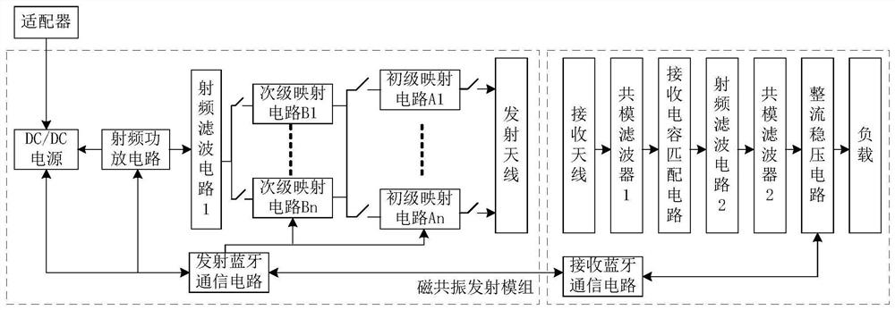
[0050] Such as figure 1 As shown, a magnetic resonance wireless charging system that suppresses system radiation and strays includes an adapter, a magnetic resonance transmitting module, and a magnetic resonance receiving module;
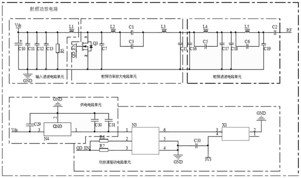
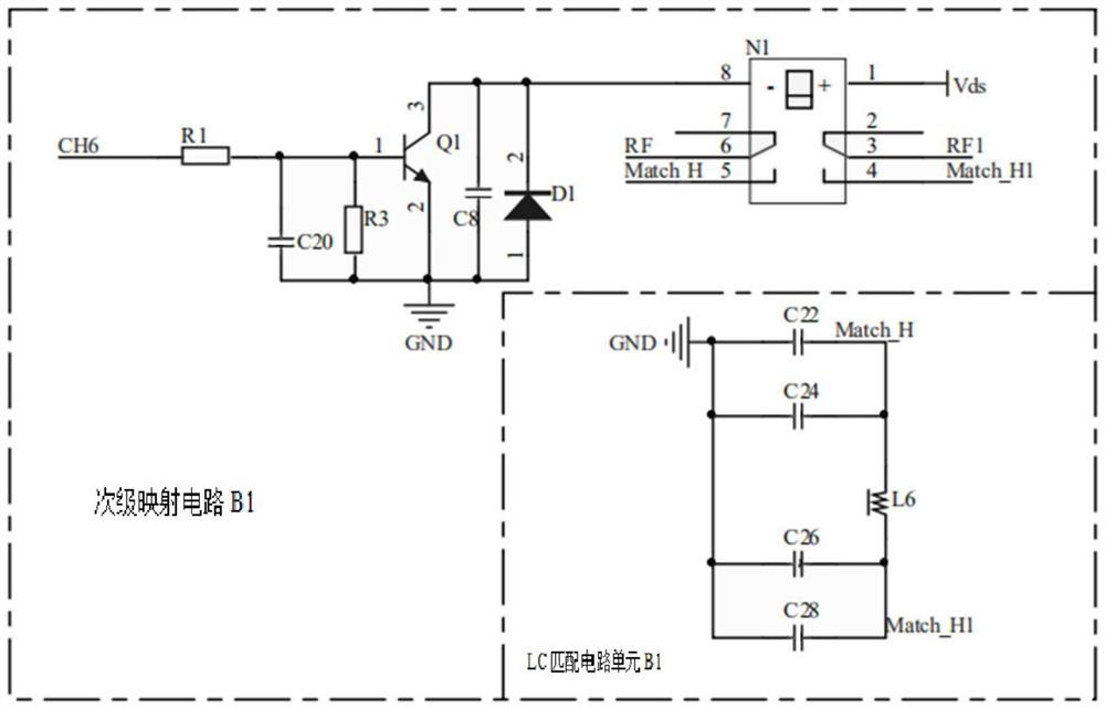
[0051] The magnetic resonance transmission module includes a DC / DC power supply, a radio frequency power amplifier circuit, a radio frequency filter circuit 1, several secondary mapping circuits composed of LC matching and capacitor matching networks, several primary mapping circuits composed of LC matching networks, and a Bluetooth transmitter A communication circuit and a transmitting antenna; the DC / DC power supply is electrically connected to the adapter, the radio frequency power amplifier circuit and the bluetooth transmission circuit respectively, the radio frequency power amplifier circuit is electrically connected to the radio frequency filter circuit 1, and the radio frequency filter circuit 1 is connected to the radio frequency filter circ...
Embodiment 2
[0089] The change of the impedance of the antenna system after the transmitting and receiving antenna passes through the primary mapping circuit A1 and the secondary mapping circuit B1 within the distance variation range of 0cm-5cm.
[0090] according to Figure 18 The schematic diagram shown, combined with the actual application requirements, adopts the following electrical parameters for this case:
[0091] Table 1: Electrical parameters when there is only a capacitor matching network in Implementation Case 2
[0092] symbol identification value C149 58pF C147 150pF C153 150pF
[0093] Table 2: Zin values measured under the electrical parameters in Table 1
[0094] distance frequency Zin 0cm 6.78Mhz 79R-23j 1cm 6.78Mhz 54R-17j 2cm 6.78Mhz 43R-10j 3cm 6.78Mhz 29R-0j 4cm 6.78Mhz 22R+3j 5cm 6.78Mhz 16R+6j
[0095] according to Figure 19 In the schematic diagram shown...
Embodiment 3
[0105] Embodiment 3: Combining the primary mapping circuit, secondary mapping circuit, and capacitor matching network of Example 2, the receiving end adopts only the capacitor matching circuit, adds a hybrid filter, and adds a primary filter and a hybrid filter.
[0106] according to Figure 21 In the schematic diagram shown, Zin is the input impedance of the antenna at the transmitting end, and ZL is the equivalent load impedance at the receiving end. Combined with the actual application requirements, the following electrical parameters are used for this case:
[0107] Table 7: The transmitting end is to add the primary mapping circuit and the secondary mapping circuit, and the receiving end only has the electrical parameters of the capacitance matching network
[0108]
[0109]
PUM
 Abstract
Description
Claims
Application Information


