
Wafer ink dot identification method

A technology of wafers and ink dots, which is applied in image data processing, instruments, calculations, etc., can solve the problems of inability to apply wafer ink dot marking, outflow of bad chips, and time-consuming, etc., so as to reduce labor costs, reduce scrapping, and improve The effect of accuracy

Pending Publication Date: 2021-06-08
SEMICON MFG ELECTRONICS (SHAOXING) CORP
View PDF0 Cites 1 Cited by
  • Summary
  • Abstract
  • Description
  • Claims
  • Application Information

AI Technical Summary

Problems solved by technology

This method of ink dot marking relies entirely on manual recording and ink dot marking by engineers, which is inefficient and time-consuming, and cannot be applied to ink dot marking of mass-produced wafers, and manual image processing is easy to make mistakes and easily cause defects Chips flow out due to missing labels, causing bad chips to flow out, resulting in low yield rate and resulting in quality claims from customers

Method used


Image

  • Wafer ink dot identification method
  • Wafer ink dot identification method
  • Wafer ink dot identification method

Examples


Embodiment Construction

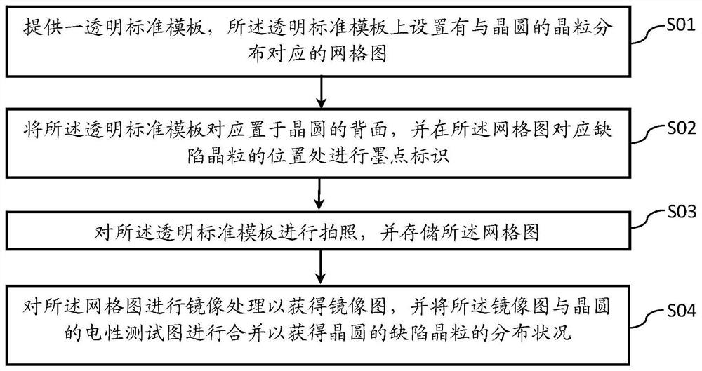
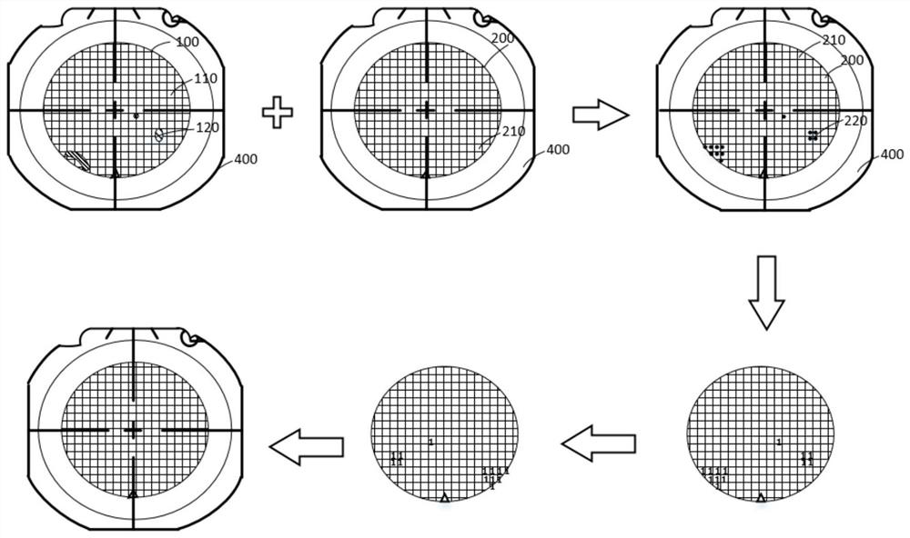
[0025] The method for marking ink dots on a wafer according to the present invention will be further described in detail below in conjunction with the accompanying drawings and specific embodiments. According to the following description and accompanying drawings, the advantages and characteristics of the present invention will be clearer, however, it should be noted that the concept of the technical solution of the present invention can be implemented in many different forms, and is not limited to the specific implementation set forth herein. example. The drawings are all in very simplified form and use imprecise scales, and are only used to facilitate and clearly assist the purpose of illustrating the embodiments of the present invention.

[0026] The terms "first", "second", etc. in the specification are used to distinguish between similar elements, and are not necessarily used to describe a specific order or chronological order. It is to be understood that the terms so us...


PUM


Abstract

The invention provides a wafer ink dot identification method, which comprises the following steps of: placing a transparent standard template on the back surface of a wafer, performing ink dot identification on defective crystal grains in a grid chart of the transparent standard template, photographing the transparent standard template to store the grid chart, performing mirror image processing on the grid chart to obtain a mirror image, And combining the mirror image with the electrical test pattern of the wafer to obtain the distribution condition of the defective crystal grains of the wafer. According to the invention, point-to-point ink dot identification of the defective crystal grains on the wafer is achieved, misjudgment caused by manual recording of the defective crystal grains is avoided, and the labor cost is reduced at the same time. Furthermore, mirror image processing is carried out on the grid chart with the coordinate information of the defective crystal grains through data processing software so as to obtain a mirror image corresponding to the distribution condition of the wafer defective crystal grains, errors caused by manual mirror image processing are reduced, meanwhile, mass production of wafer ink dot marks is achieved, the accuracy of wafer ink dot marking is improved, and scrap of crystal grains is reduced.

Description

technical field [0001] The invention relates to the field of integrated circuit manufacturing, in particular to a method for marking ink dots on a wafer. Background technique [0002] In semiconductor production, as the size of the wafer increases and the size of the components shrinks, a wafer can be divided into thousands of identical or different chips as required. Due to the process design or the characteristics of the material itself, there are defective dies (Defect Die) and qualified dies (Good Die) on the final wafer. Generally, a test machine and a probe card (ProbeCard) are used to test each die on the wafer to ensure that the electrical characteristics and performance of the die meet the design specifications. If a defective grain is found during the test, it needs to be marked. Specifically, ink can be applied to the defective grain for ink dot marking (Ink) for subsequent delineation and packaging. [0003] For NTO (New Tape-out, new products), it is necessary...

Claims


Application Information

Patent Timeline
IPC IPC(8): G06T7/00
CPCG06T7/001G06T7/0008G06T2207/30148
Inventor 高冰玲
Owner SEMICON MFG ELECTRONICS (SHAOXING) CORP
Learn More