Gas sensor and manufacturing method thereof
A gas sensor and metal electrode technology, applied in the field of sensors, can solve the problems of slow desorption process, poor selectivity, limited gas response sensitivity, etc., to improve specific selectivity, realize room temperature detection, and flexible response strength and response selectivity. Effect
- Summary
- Abstract
- Description
- Claims
- Application Information
AI Technical Summary
Problems solved by technology
Method used
Image
Examples
Embodiment 1
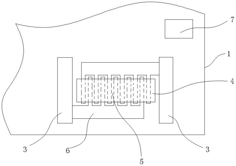
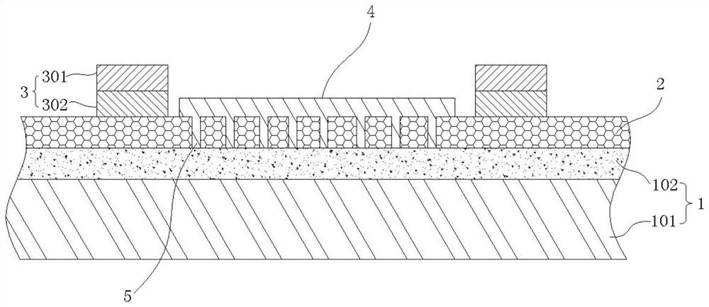
[0032] Specifically, such as figure 1 As shown, the gas sensor of the present embodiment includes a substrate 1, a graphene layer 2, a metal electrode pair, and a metal oxide layer 4; the substrate 1, the graphene layer 2, and the metal electrode pair are arranged sequentially from bottom to top; a metal electrode pair Including two metal electrodes 3, the area between the two metal electrodes 3 of a metal electrode pair is a channel;
[0033] The graphene layer 2 at the channel is provided with a gap groove 5, so that the graphene layer 2 at the channel is disconnected to form a graphene electrode pair; the metal oxide layer 4 is located at the channel and covers the graphene electrode On the pair and gap groove 5, to connect the graphene electrode pair, the metal oxide layer 4 of the present embodiment is covered in the central region of the graphene electrode pair; The area of the metal oxide layer 4 is less than the area of the channel, so that in the channel It has a...
Embodiment 2
[0040] Specifically, such as Figures 2 to 3 As shown, in the gas sensor of this embodiment, the thickness of the silicon dioxide layer 102 of this embodiment is 90 nm. The width of the gap groove 5 in this embodiment is 200 nm. The metal oxide layer 4 in this embodiment is a copper oxide layer. The metal material is deposited by photolithography and electron beam evaporation; the thickness of the metal material is 5nm in this example. In this embodiment, the thickness of the chromium layer 302 is 3 nm, and the thickness of the gold layer 301 is 6 nm. In this embodiment, the distance between the two metal electrodes 3 is 2mm.
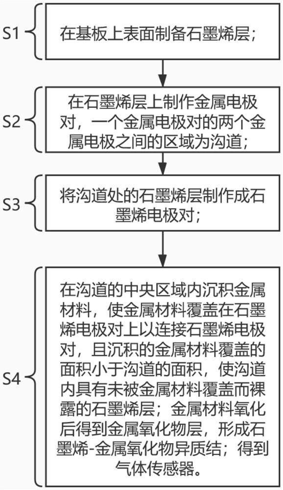
[0041] This embodiment 2 also provides a method for manufacturing the above-mentioned gas sensor. The manufacturing material includes the substrate 1, including the following steps:
[0042] Step S1, preparing a graphene layer 2 on the upper surface of the substrate 1;
[0043] Step S2, making metal electrode pairs on the graphene layer 2, the area...
PUM
| Property | Measurement | Unit |
|---|---|---|
| thickness | aaaaa | aaaaa |
| thickness | aaaaa | aaaaa |
| thickness | aaaaa | aaaaa |
Abstract
Description
Claims
Application Information


