Optical detector with superstructure surface coupled with transverse thermoelectric film and manufacturing method
A technology of transverse pyroelectric and optical detectors, applied in the direction of electric radiation detectors, etc., can solve the problems of inability to achieve spectral selective response, low sensitivity of mid- and far-infrared light, etc., and achieve the effect of simple structure and fast response
- Summary
- Abstract
- Description
- Claims
- Application Information
AI Technical Summary
Problems solved by technology
Method used
Image
Examples
Embodiment 1
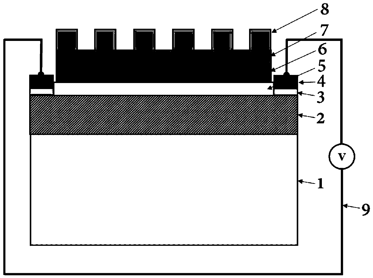
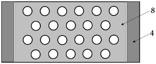
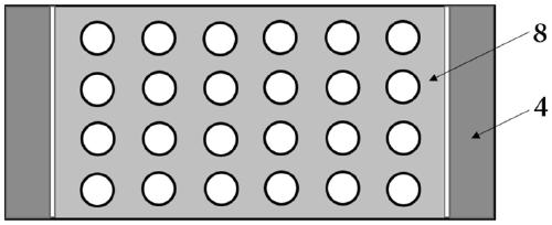
[0050] This embodiment discloses a photodetector with a superstructure surface coupled to a transverse pyroelectric thin film. The superstructure surface is coupled to the transverse pyroelectric thin film 2 through an intermediate insulating layer 5. The structure of the formed detector is as follows figure 1 As shown, the detector includes: an oblique substrate 1, and a lateral pyroelectric thin film 2 epitaxially grown on the oblique substrate 1, the surface normal direction of the oblique substrate 1 is relative to the crystal of the substrate 1 There is an inclination angle in the direction of 5°-30°, and the lattice of the substrate 1 matches the lattice of the lateral thermoelectric thin film 2. At both ends of the surface of the lateral thermoelectric film 2 along the oblique direction of the substrate, a Ti film (or Cr film) bonding layer 3 with a thickness of 5 nm is deposited first, and then an 80 nm thick Au film electrode coating is deposited on the bonding layer....
Embodiment 2
[0053] This embodiment is based on the first embodiment, and discloses a photodetector with a superstructured surface coupled with a transverse pyroelectric thin film 2. The metal thin film with a superstructured surface and the dielectric layer form an infrared light absorber, which is directly deposited on the A mid-to-far infrared photodetector is formed on the surface of the lateral pyroelectric film 2, and its structure is as follows: Figure 6 As shown, the detector includes: an oblique substrate 1, and a lateral pyroelectric thin film 2 epitaxially grown on the oblique substrate. Similarly, the surface normal direction of the oblique substrate is relative to the crystal of the substrate 1. There is an inclination angle in the direction of 5°-30°, and the lattice of the substrate 1 matches the lattice of the lateral thermoelectric thin film 2. At both ends of the lateral thermoelectric thin film 2, a bonding layer 3 of a Ti film (or Cr film) with a thickness of 5 nm is ...
Embodiment 3
[0056] This embodiment is based on a method of using a photodetector with a superstructure surface coupled with a transverse pyroelectric thin film 2 in Embodiments 1 and 2, such as Figure 7 As shown, the continuous infrared light is incident on the infrared detector 18 after passing through the chopper 17, and the optical signal is converted into an electrical signal output, and the magnitude of the electrical signal is recorded by a lock-in amplifier; the pulsed infrared light can directly heat the infrared detector 18 , to generate a time-resolved voltage signal that is acquired by an oscilloscope.
PUM
| Property | Measurement | Unit |
|---|---|---|
| Thickness | aaaaa | aaaaa |
| Thickness | aaaaa | aaaaa |
| Thickness | aaaaa | aaaaa |
Abstract
Description
Claims
Application Information


