A Structure Design for Improving the Sensitivity of Mos2 Thin Film Field Effect Transistor Gas Sensor

A gas sensor and thin film field effect technology, applied in the direction of material resistance, can solve the problems that limit the development of low-power gas sensing, and achieve the effects of enhanced room temperature gas-sensing effect, high surface activity, and excellent conductivity

Active Publication Date: 2021-08-10
CHINA JILIANG UNIV
View PDF10 Cites 0 Cited by
  • Summary
  • Abstract
  • Description
  • Claims
  • Application Information

AI Technical Summary

Problems solved by technology

In 2012, the Institute of Nanotechnology of the Karlsruhe Institute of Technology in Germany reported for the first time about the thin film field effect transistor of tin oxide, and the mobility of the device prepared by a simple spin-coating process can reach 0.13cm 2 V -1 the s -1 , the switching ratio is 85, and the threshold voltage is -1.9V, but it also requires a higher gate voltage (above -50V) and source and drain voltage (-90V) as well as a harsh experimental environment (test in an inert atmosphere) to Fully realize high mobility; the harsh conditions required for high mobility also objectively limit the development of low-power gas sensing in practical applications, so this technology has not been used to detect gases
However, these traditional single bare FET sensors usually require large external gate bias to achieve high sensitivity
What's more, even at high gate bias, the response and recovery times are slow for practical applications

Method used


Image

  • A Structure Design for Improving the Sensitivity of Mos2 Thin Film Field Effect Transistor Gas Sensor
  • A Structure Design for Improving the Sensitivity of Mos2 Thin Film Field Effect Transistor Gas Sensor
  • A Structure Design for Improving the Sensitivity of Mos2 Thin Film Field Effect Transistor Gas Sensor

Examples


Embodiment Construction

[0030] In order to make the object, technical solution and advantages of the present invention more clear, the present invention will be further described in detail below in conjunction with the accompanying drawings and embodiments.

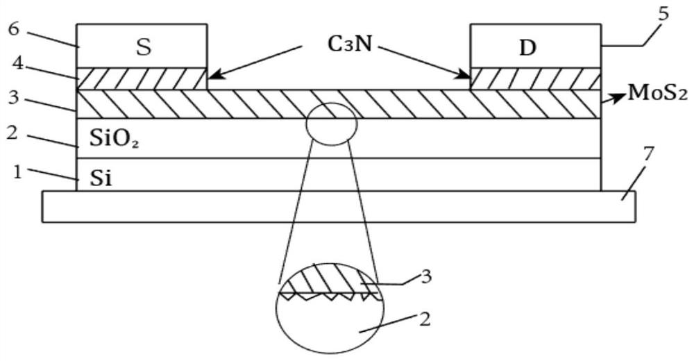
[0031] The MoS-based 2 Thin film field effect transistor gas sensors (such as figure 1 shown), including: substrate (1), gate insulating layer (2), channel active layer (3), 2DC 3 N electrode deposition carrier (4), source electrode (6) and drain electrode (5), and grid (7) made of indium tin oxide (commonly known as ITO) film transparent conductive glass.

[0032] The preparation method can adopt the following steps: use chemical vapor deposition (CVD) to deposit a single layer of MoS 2 The thin film is deposited on a silicon-based substrate to form a channel active layer, where a gate insulating layer is pre-deposited on the silicon-based substrate, and undergoes ion etching and HF wet etching; a single-layer two-dimensional material (2D) C ...


PUM


Abstract

The invention discloses an improved MoS-based 2 Structural Design Method for Sensitivity of Thin Film Field Effect Transistor Type Gas Sensor. The structure includes substrate, gate insulating layer, channel active layer, source, drain and gate. The substrate material of the present invention is silicon, on which the gate electrode is drawn. Channel active layer is MoS 2 quantum dot film. Add two-dimensional material (2D) C on the source and drain electrode regions 3 N, with MoS 2 Forming a heterojunction reduces the height of the Schottky barrier. An active electrode and a drain electrode are deposited on the heterojunction, and the material is gold. The insulating layer material is SiO 2 , by designing nanoscale ripples and peaks on the surface to induce a local strain field, compared with conventional devices, the carrier mobility in the film increases by two orders of magnitude. When the measured gas molecules touch the quantum dot film, the internal carrier concentration will change. Through voltage regulation, the majority of carriers will be transported in a directional manner, forming a loop current, and the current value changes before and after passing through the gas to achieve low concentration detection. The role of gas.

Description

technical field [0001] The invention belongs to the technical field of gas sensors, and more specifically relates to a structure design of a thin film field effect transistor type gas sensor. The gas sensor is based on a single-layer MoS 2 Thin film field effect transistor type gas sensor with thin film as gas sensitive layer. Background technique [0002] Traditional semiconductor gas sensors are usually based on gas-sensitive materials (such as SnO 2 , TiO 2 etc.) when in contact with gas, the resistance value changes to achieve the effect of gas detection. It has the characteristics of simple measurement method, high sensitivity, fast response, convenient operation, good portability, and low cost. However, this type of gas sensor generally adopts mature technology but Relatively large tubular or chip ceramic substrates, and commercial sensors must work at higher operating temperatures (200-600°C), resulting in higher power consumption, which reduces the portability and ...

Claims


Application Information

Patent Timeline
Patent Type & Authority Patents(China)
IPC IPC(8): G01N27/12
Inventor 李泽南金尚忠金怀洲严永强张益溢赵春柳石岩赵天琦周亚东
Owner CHINA JILIANG UNIV
Why Eureka
Try Eureka