Gallium nitride-based power device epitaxial structure and production method thereof

A technology of epitaxial structures and power devices, applied in semiconductor/solid-state device manufacturing, semiconductor devices, electrical components, etc., can solve the problems of high Al composition in non-gate regions and unsatisfactory Al composition in gate regions

Inactive Publication Date: 2021-06-18
HUNAN SANAN SEMICON CO LTD
View PDF5 Cites 0 Cited by
  • Summary
  • Abstract
  • Description
  • Claims
  • Application Information

AI Technical Summary

Problems solved by technology

However, the existing epitaxial structure is usually an AlGaN barrier layer with a single aluminum composition, so it cannot meet the requirements of low Al composition in the gate region and high Al composition in the non-gate region

Method used


Image

  • Gallium nitride-based power device epitaxial structure and production method thereof
  • Gallium nitride-based power device epitaxial structure and production method thereof
  • Gallium nitride-based power device epitaxial structure and production method thereof

Examples


no. 1 example

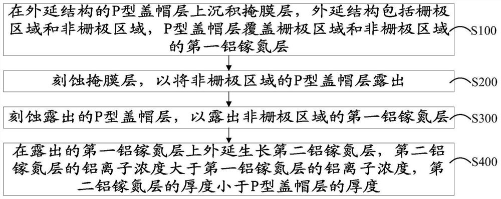
[0042] Please refer to figure 1 , this embodiment provides a method for preparing an epitaxial structure of a gallium nitride-based power device, and the method for preparing the epitaxial structure of a gallium nitride-based power device includes:

[0043] S100, depositing a mask layer 20 on the P-type cap layer 15 of the epitaxial structure, the epitaxial structure includes a gate region and a non-gate region, and the P-type cap layer 15 covers the first AlGaN in the gate region and the non-gate region Layer 14.

[0044] It should be noted that please refer to Figure 5 As shown, the above-mentioned epitaxial structure includes a substrate 11 , and a nucleation layer, a buffer layer 12 , a channel layer 13 , a first AlGaN layer 14 , and a P-type capping layer 15 sequentially formed on the substrate 11 . Wherein, the above-mentioned substrate 11 can be a silicon substrate, the buffer layer 12 and the channel layer 13 can be a gallium nitride layer, the first aluminum galliu...

no. 2 example

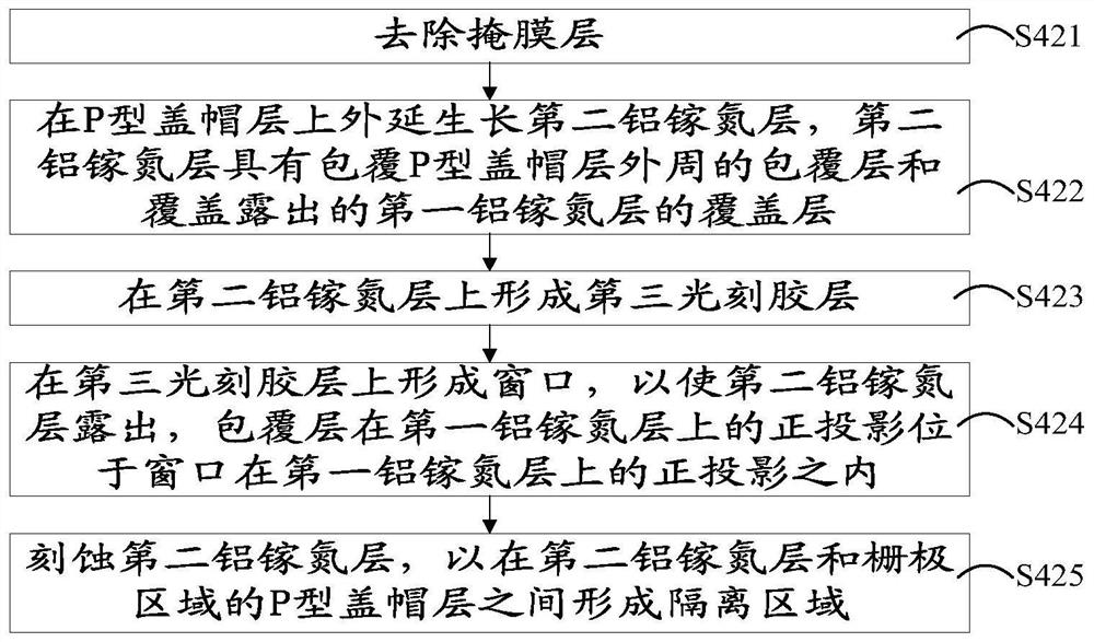
[0091] Compared with the first embodiment, this embodiment differs in that the mask layer 20 is made of SiO 2 layer (or SiN, Al 2 o 3 , HfO 2 Any one of them) is replaced by a photoresist layer. In this way, the method for preparing the epitaxial structure of a GaN-based power device provided in this embodiment will undergo adaptive changes.

[0092] In this way, the method for preparing the epitaxial structure of a gallium nitride-based power device should be prepared according to the following principle: that is, first deposit a photoresist layer on the P-type capping layer 15 of the epitaxial structure, such as Figure 5 shown; and then by exposure and development, remove the photoresist layer in the non-gate region, to expose the P-type capping layer 15 in the non-gate region, as Image 6 shown; and then etch the P-type capping layer 15 to expose the first AlGaN layer 14 located in the non-gate region, as Figure 7 shown; then remove the photoresist layer, and epitaxi...


PUM

PropertyMeasurementUnit
thicknessaaaaaaaaaa
thicknessaaaaaaaaaa

Abstract

The invention provides a gallium nitride-based power device epitaxial structure and a production method thereof, and relates to the technical field of semiconductors. The method comprises the steps of depositing a mask layer on a P-type cap layer of an epitaxial structure, wherein the epitaxial structure comprises a gate region and a non-gate region, and the P-type cap layer covers first aluminum gallium nitride layers of the gate region and the non-gate region; etching the mask layer to expose the P-type cap layer in the non-gate region; etching the exposed P-type cap layer to expose the first aluminum gallium nitride layer in the non-gate region; and epitaxially growing a second aluminum gallium nitride layer on the exposed first aluminum gallium nitride layer, wherein the aluminum ion concentration of the second aluminum gallium nitride layer is greater than that of the first aluminum gallium nitride layer, and the thickness of the second aluminum gallium nitride layer is smaller than that of the P-type cap layer. According to the production method of the gallium nitride-based power device epitaxial structure , the aluminum component in the gate region of the barrier layer is low, the aluminum component in the non-gate region is high, the threshold voltage of the device and the reliability of the gate are improved, an on-resistance is reduced, and the performance of the device is improved.

Description

technical field [0001] The invention relates to the technical field of semiconductors, in particular to an epitaxial structure of a gallium nitride-based power device and a preparation method thereof. Background technique [0002] Gallium nitride is a typical representative of the third-generation wide bandgap semiconductor material. Due to its large bandgap, high critical breakdown electric field and high electron saturation velocity, gallium nitride is widely used in broadband communication, power electronics and other fields. widely used. Among them, the most widely used one is the High Electron Mobility Transistor (HEMT). [0003] In the prior art, enhancement-mode gallium nitride-based high electron mobility transistors are mainly manufactured through the following methods: recessed gate structure, fluorine ion implantation technology, and p-type capping layer technology. Among them, the p-type cap technology is currently the most commonly used method to achieve indus...

Claims


Application Information

Patent Timeline
Patent Type & Authority Applications(China)
IPC IPC(8): H01L29/06H01L29/20H01L29/423H01L29/778H01L21/335
CPCH01L29/0603H01L29/2003H01L29/42316H01L29/66462H01L29/778
Inventor 梁玉玉蔡文必何俊蕾刘成叶念慈
Owner HUNAN SANAN SEMICON CO LTD
Why Eureka
Try Eureka